Introduction to PCB Layers
Printed Circuit Boards (PCBs) are essential components in modern electronics, providing a platform for mounting and interconnecting electronic components. A PCB consists of multiple layers, each serving a specific purpose in the overall functionality of the board. Among these layers, the outer layer, also known as the surface layer or top and bottom layers, plays a crucial role in the PCB’s design and performance.
In this comprehensive article, we will delve into the intricacies of the Outer PCB Layer, exploring its characteristics, manufacturing processes, and the various considerations that go into its design. By the end of this article, you will have a thorough understanding of the outer PCB layer and its significance in the world of electronics.
The Importance of the Outer PCB Layer
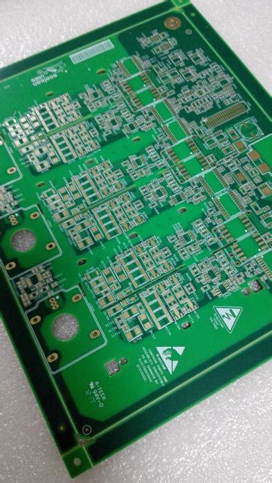
The outer PCB layer is the topmost and bottommost layer of a PCB, making it the most visible and accessible part of the board. Its importance lies in several key aspects:
- Component Placement: The outer layer is where most of the electronic components, such as resistors, capacitors, and integrated circuits, are mounted. The proper placement and orientation of these components on the outer layer are crucial for the PCB’s functionality and efficiency.
- Electrical Connectivity: The outer layer features conductive traces and pads that connect the various components on the board. These traces are carefully designed to ensure optimal signal integrity and minimize interference.
- Protection and Durability: The outer layer serves as a protective barrier for the inner layers of the PCB. It is often coated with a solder mask, which insulates the conductive traces and prevents short circuits. Additionally, silkscreen printing on the outer layer provides labels and markings for easy identification of components and orientation.
Characteristics of the Outer PCB Layer
To fully comprehend the outer PCB layer, it is essential to understand its key characteristics:
Material Composition
The outer layer of a PCB is typically made of copper, which is an excellent conductor of electricity. The copper layer is laminated onto a substrate material, such as FR-4, which provides insulation and mechanical support. The thickness of the copper layer can vary depending on the specific requirements of the PCB, with common thicknesses ranging from 0.5 oz to 2 oz per square foot.
Solder Mask
The solder mask is a thin, protective layer applied over the copper traces on the outer layer. Its primary purpose is to insulate the conductive traces and prevent short circuits during the soldering process. The solder mask is typically green in color, but other colors, such as red, blue, or black, can also be used for specific applications or aesthetic purposes.
Silkscreen
Silkscreen is the process of printing text, logos, and other markings on the outer layer of the PCB. It is usually done in white color and provides important information such as component designators, polarity indicators, and company logos. The silkscreen helps in the assembly process and makes it easier to identify components and their orientation.
Surface Finish
The surface finish is a protective coating applied to the exposed copper on the outer layer of the PCB. Its purpose is to prevent oxidation and enhance the solderability of the copper pads. There are several types of surface finishes available, each with its own advantages and disadvantages. Some common surface finishes include:
- Hot Air Solder Leveling (HASL)
- Organic Solderability Preservative (OSP)
- Electroless Nickel Immersion Gold (ENIG)
- Immersion Silver (IAg)
- Immersion Tin (ISn)
The choice of surface finish depends on factors such as the intended application, environmental conditions, and cost considerations.

Manufacturing Process of the Outer PCB Layer
The manufacturing process of the outer PCB layer involves several steps, each requiring precision and attention to detail. Let’s take a closer look at these steps:
- Copper Lamination: The process begins with the lamination of a thin layer of copper onto the substrate material. The copper foil is bonded to the substrate using heat and pressure, creating a strong and stable base for the subsequent steps.
- Drilling: Holes are drilled through the PCB to accommodate through-hole components and to create vias that connect different layers of the board. The drilling process is performed using high-speed, computer-controlled drilling machines.
- Patterning: The desired circuit pattern is transferred onto the outer layer using a photolithography process. A photoresist layer is applied to the copper surface, and then the circuit pattern is exposed using UV light. The exposed areas of the photoresist are then removed, leaving behind a protective mask for the etching process.
- Etching: The unwanted copper is removed from the outer layer using a chemical etching process. The exposed copper is dissolved, leaving behind the desired circuit pattern protected by the photoresist mask.
- Solder Mask Application: A solder mask layer is applied over the etched copper traces to provide insulation and protection. The solder mask is typically applied using a silkscreen printing process, and then it is cured using UV light.
- Silkscreen Printing: The silkscreen printing process is used to apply text, logos, and other markings onto the outer layer of the PCB. The silkscreen ink is applied through a fine mesh screen, and then it is cured using heat.
- Surface Finish Application: The chosen surface finish is applied to the exposed copper pads on the outer layer. The specific application process varies depending on the type of surface finish being used.

Design Considerations for the Outer PCB Layer
Designing the outer PCB layer requires careful consideration of various factors to ensure optimal performance and manufacturability. Some key design considerations include:
Component Placement
The placement of components on the outer layer should be optimized for signal integrity, thermal management, and ease of assembly. Components should be placed in a logical and organized manner, with sufficient spacing between them to prevent interference and facilitate soldering.
Trace Routing
The routing of conductive traces on the outer layer should be done in a way that minimizes signal interference and ensures proper electrical connectivity. Trace width and spacing should be carefully calculated based on the signal requirements and the PCB’s intended application.
Solder Mask Design
The solder mask design should be optimized to provide adequate insulation and protection for the conductive traces while allowing for proper soldering of components. Solder mask openings should be sized appropriately to ensure good solder joint formation and prevent solder bridging.
Silkscreen Design
The silkscreen design should be clear, legible, and properly aligned with the components and traces on the outer layer. The silkscreen should provide necessary information for assembly and troubleshooting without obscuring important features of the PCB.
Design for Manufacturing (DFM)
The outer layer design should adhere to the principles of Design for Manufacturing (DFM) to ensure that the PCB can be efficiently and reliably manufactured. This includes considerations such as minimum trace widths, pad sizes, and clearances, as well as the selection of appropriate surface finishes and solder mask materials.
Frequently Asked Questions (FAQ)
- What is the purpose of the solder mask on the outer PCB layer?
The solder mask serves as an insulating and protective layer over the copper traces on the outer layer. It prevents short circuits during the soldering process and provides a barrier against environmental factors such as moisture and contamination. - How does the choice of surface finish affect the performance of the outer PCB layer?
The choice of surface finish can impact the solderability, durability, and electrical performance of the outer PCB layer. Different surface finishes have varying properties in terms of oxidation resistance, shelf life, and compatibility with different soldering processes. The selection of the appropriate surface finish depends on the specific requirements of the PCB and its intended application. - What is the significance of silkscreen printing on the outer PCB layer?
Silkscreen printing is used to apply text, logos, and other markings on the outer layer of the PCB. It provides important information for assembly and troubleshooting, such as component designators, polarity indicators, and company branding. The silkscreen helps in the identification of components and their orientation, making the assembly process more efficient and reducing the likelihood of errors. - What are some common design challenges associated with the outer PCB layer?
Some common design challenges associated with the outer PCB layer include: - Ensuring proper signal integrity and minimizing interference between traces
- Optimizing component placement for thermal management and ease of assembly
- Achieving the right balance between trace width, spacing, and manufacturability
- Designing solder mask and silkscreen layouts that are clear, accurate, and compliant with manufacturing constraints
- Selecting the appropriate surface finish based on the PCB’s requirements and cost considerations
- How does the outer PCB layer differ from the inner layers in terms of design and manufacturing?
The outer PCB layer differs from the inner layers in several ways: - The outer layer is the most visible and accessible part of the PCB, while the inner layers are hidden within the board.
- The outer layer is where most of the components are mounted and soldered, while the inner layers primarily contain interconnects and power/ground planes.
- The manufacturing process for the outer layer involves additional steps such as solder mask application, silkscreen printing, and surface finish application, which are not required for the inner layers.
- The design considerations for the outer layer, such as component placement, trace routing, and silkscreen design, are often more critical and complex compared to the inner layers.
Conclusion
The outer PCB layer is a critical component of a printed circuit board, serving multiple functions such as component placement, electrical connectivity, and protection. Understanding the characteristics, manufacturing processes, and design considerations associated with the outer layer is essential for creating high-quality and reliable PCBs.
From the material composition and solder mask application to the silkscreen printing and surface finish selection, each aspect of the outer layer plays a crucial role in the overall performance and manufacturability of the PCB. By carefully considering factors such as component placement, trace routing, and Design for Manufacturing (DFM) principles, PCB designers can optimize the outer layer design to meet the specific requirements of their applications.
As PCB technology continues to evolve, the importance of the outer layer remains paramount. Advancements in materials, manufacturing processes, and design tools will further enhance the capabilities and reliability of the outer PCB layer, enabling the development of increasingly complex and sophisticated electronic devices.
By delving into the intricacies of the outer PCB layer, we gain a deeper appreciation for the engineering and craftsmanship that goes into creating these essential components. From the simplest single-layer boards to the most advanced multi-layer designs, the outer layer stands as a testament to the ingenuity and precision of the electronics industry.


Leave a Reply