Printed circuit boards (PCBs) and printed circuit board assemblies (PCBAs) are crucial components in electronics, but the terms are sometimes used incorrectly. Understanding the distinction between PCB and PCBA aids communication across product design and manufacturing. This article clarifies the unique meanings to distinguish bare boards from assembled boards containing electronics components.
Definitions
PCB stands for printed circuit board – the bare circuit board without integrated components.
Whereas PCBA denotes printed circuit board assembly – a production-ready board stuffed with electronics parts ready for application.
Another definition is:
PCB – Rigid laminated board structure with etched conductive copper tracing to provide electrical interconnections.
PCBA – PCB populated with leaded or surface mount components soldered in place constituting a functional electronic circuit or sub-assembly.
| Term | Definition |
|---|---|
| PCB | Printed Circuit Board<br>(Bare board without components) |
| PCBA | Printed Circuit Board <br>Assembly <br>(Board with soldered components) |
Table: Summary of key terminology
So in brief, the central distinction is:
- PCB = Bare board
- PCBA = Circuit board plus components
The following sections explore PCB and PCBA aspects deeper.
What is a PCB?
A printed circuit board or PCB provides a structural foundation for mounting and interconnecting electronic components using conductive pathways etched from copper sheets laminated onto an insulating non-conductive base.
As per the IPC-2221A standard, the generic PCB construction comprises:
- Conductive layers – Copper tracks to channel signals between attached components.
- Dielectric layers – Insulating substrate to separate copper layers preventing short circuits while holding layers together. Common materials are FR-4 fiberglass, ceramic or polyimide.
- Vias – Plated through holes linking conductive layers to enable vertical interconnection between layers. Microvias achieve higher component densities.
- Pads & traces – Copper regions allow component pins or leads to structurally attach and electrically join to tracks routing signals the circuit layout.
- Solder mask – Epoxy layer over copper prevents solder bridges while leaving pads exposed for connections. Often color coded green, red, yellow, black, blue etc.
- Silkscreen – White epoxy ink applied to print reference designators, polarity markers, logos or text for board identification without affecting function. Also prevents solder bridging.
- Edge connectors – Gold plated protruding fingers enable plugging into mating interfaces for extending connectivity.
- Surface finish – Coating preventing oxidation ensuring reliable soldering. Common finishes are organic solderability preservative (OSP), immersion silver, electroless nickel immersion gold (ENIG) and immersion tin.
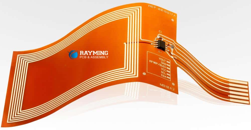
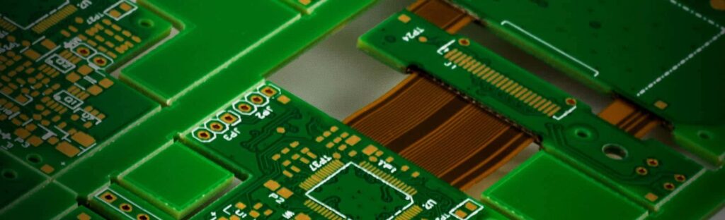
While 99% of PCBs are rigid, some applications utilize flexible PCB construction allowing bending and twisting tolerant of flexing stresses. Regardless of type, the term PCB implies an unpopulated board containing only conductive layers, insulating substrate and plating. Mounting components occurs later during PCB assembly (PCBA).
What is PCBA?
Printed circuit board assembly or PCBA adds electronic components onto a PCB to deliver functionality forming an electronic subassembly or complete product. This contrasts to the raw PCB which only offers connection capability.
A fully loaded PCBA comprises:
- PCB – Base board with etched conductive tracks and pads.
- Components – Various surface mount (SMT) or through-holeelectronic parts soldered to pads connecting functionally together. Common types are resistors, capacitors, ICs, transistors, LEDs, integrated circuits, connectors etc.
- Solder joints – Electrically and mechanically affix components to pads. Solder paste applied during assembly reflows when heated to produce reliable intermetallic connection.
- Conformal coating – Optional epoxy layer applied over the assembly for protection against moisture, dust contamination or mechanical stresses that can compromise reliability.
- Thermal solutions – Heat sinks, fans or thermal interface material aid cooling and heat dissipation especially for high power designs.
- Stenciled markings – Identifying product details, ratings, warnings and other notation used externally.
- Housings/enclosures – Protect delicate circuitry and isolate electrical hazards to ensure safety compliance.
In summary, PCB refers to bare circuit boards, whereas PCBA indicates fully stuffed boards including mounted and soldered components producing functionality.
Key Differences Between PCB and PCBA
While related, clarifying distinctions between PCB and PCBA aids technical discussion.
| Comparison | PCB | PCBA |
|---|---|---|
| Composition | Bare board | Board + components |
| Conductivity | Copper traces for connectivity | Adds mounted components |
| Function | Physical support and electrical routing framework | Functional electronics assembly |
| Process | PCB fabrication | PCB fabrication + component assembly |
| Lead time | Shorter | Longer |
| Value | Lower material cost | Higher value from components + assembly labor |
| Failure modes | Structural | Structural + component + solder joint |
Table: Key differences when contrasting PCBs and PCBAs
In summary:
- PCBs – Provide strictly conductive traces and pads without functionality
- PCBAs – Deliver functional electronics through mounted and connected components
Communicating this clearly avoids ambiguity when discussing bare boards versus assembled boards.
PCB Design and Fabrication
The starting point for all PCBA production is designing and fabricating the foundational bare circuit board or PCB.
PCB Design Process
PCB layout involves:
- Schematic capture – Draw circuit diagrams using ECAD software representing components as symbols with interconnects.
- PCB layout – Convert schematic into physical board geometry showing component footprints/pads with etched copper tracks linking contacts.
- Routing – Automatically or manually route connections on layers respecting clearance rules.
- Verification – Use design rule checks and simulation to verify signal timing, power delivery and electromagnetic compatibility.
- Documentation – Generate manufacturing Gerber files, drill tables, assembly drawings and bill of materials specifying components.
Skills spanning electronics, drafting and computing aid progression from concept circuit to manufactured bare board.
PCB Fabrication
PCB prototyping leverages various small-scale methods before advancing to volume production using specialized PCB fabrication processes.
Mass PCB Production incorporates:
- Multi-layer board construction
- Printed and etched copper foil circuitry
- Automated component population
- Volume soldering techniques
Numerous intricate steps transform raw materials into consistent reliable bare boards:
- Layer stacking glues dielectric and conductive foils
- Laser direct imaging transfers layouts
- Etching patterns copper traces
- Plating coats traces enabling soldering
- Automated optical inspection validates quality
- Panel separation divides boards
Combining engineering expertise with precision manufacturing equipment enables cost-effective volume PCB creation.
PCBA Manufacturing Stages
Constructing a working electronics product from PCBs requires PCB assembly (PCBA) through placement and attachment of components.
Major PCBA manufacturing phases comprise:
- Sourcing components – Procure approved functional parts defined on bill of materials.
- Solder paste printing – Dispense precise paste deposits onto pads.
- Pick and place – Robotically position components on pads.
- Reflow soldering – Fuse parts in place heating multiple boards in convection oven.
- Cleaning – Remove post-soldering residues.
- Automated optical inspection – Scan boards checking assembly and solder joint quality against tolerances.
- Testing & commissioning – Validate boards function electrically before system integration.
- Conformal coating – Apply protective epoxy layer for boosted reliability.
PCB assembly requires expertise in production engineering spanning procurement, processing and quality assurance.
Benefits of Contract Manufacturing Services
Many electronic products developers lacking specialized skills or scale outsource fabrication and assembly to contract manufacturers. External production offers quality, cost and speed advantages.
Contract manufacturing services offer:
- Established fabrication and assembly workflows
- Advanced SMT lines and soldering technologies
- Flexible low, medium and high volume production
- Skilled technicians performing delicate hand assembly
- Automated optical inspection checking every joint
- Environmental stress testing equipment
- Support beginning early in design process ensuring manufacturability
- Supply chain logistics smoothing procurement and inventory
These capabilities simplify launching end products while companies concentrate on core design differentiation and marketing strengths. From prototype builds through mass production ramp up, leveraging existing infrastructure minimizes costs and lead times while benefiting quality. Through strategic make versus buy trade-offs, internal efforts focus on where greater value arises.
Accordingly, both technology startups and multinationals routinely outsource production volume requirements and capacity spikes to specialists. Rather than maintaining underutilized assets, customizable solutions from manufacturing partners scale flexibly on demand.
FQA on PCB and PCBA
Clarifying frequently asked questions further distinguishes between PCB and PCBA:
Can a PCB Become a PCBA? {h4}
Yes absolutely, every PCBA begins life as a blank PCB. Upon applying solder paste then populating components atop pads using pick and place machines, reflow soldering bonds parts onto boards creating assemblies. Defective solder joins get reworked by hand ensuring reliable electrically and mechanically robust connections. Further production line steps incorporate inspection, test and protection coatings to furnish fully functional assemblies.
What Testing is Performed on Bare PCBs vs Assembled PCBAs? {h4}
Bare PCBs undergo:
- Dimensional inspection – Confirms physical board size, hole positions and distances between features lie within prescribed ranges.
- Netlist testing – Verifies electrical connectivity between copper pads/traces is continuity compliant matching schematic.
Whereas PCBAs require:
- In-circuit testing – Electrical probes actively energize assembled boards checking voltage and signals at key nets evaluating functional performance against broadband specifications.
- Burn-in testing – Units get powered continually over days determining infant mortality failure rates indicating component and solder joint robustness.
As PCBs lack components, functional validation applies only during PCBA checking plus broader lifecycle and environmental stress testing.
Can a Damaged PCBA become a PCB Again? {h4}
If assembled boards fail during testing, diagnosis localizes which components and joints exhibit deficiencies. Precision rework tools then detach faulty parts converting assemblies back into reusable PCBs. Common rework methods encompass:
- Desoldering – Applying heat dismantles weak joint connections to liberate components
- Jig grinding – Mechanical abrasion removes residual solder
- Laser depaneling – Precision beams cut around components for clean removal
Skillful technicians transform once populated boards into bare PCBs for fresh assembly attempting to rescue functional boards. However thermal or mechanical damage may render some beyond further restoration as PCBs. When unrecoverable, boards get scrapped to reclaim materials.
Can PCB Designs be Converted to Flexible Boards? {h4}
If product goals value flexibility, curved forms or dynamic bending stresses, flexible PCBs substitute traditional rigid fiberglass substrates with thin polyimide films allowing moderate flexing without compromise. Alterations adapt rigid PCB layouts:
- Narrower tracks withstand flexing strains
- Flex-cuts selectively weaken areas enabling controlled folds
- Strain relief patterns guide stresses safely
- Adhesives tack layers enhancing durability
However for signals above 10-20MHz, controlled impedances get disrupted losing integrity. Where high frequency response remains vital, hybrid designs integrate minimal flexibility while retaining thicker rigid sections for RF and high-speed components. With consideration for mechanical and electrical implications, many PCB products transition onto flex circuitry gaining 3D packaging efficiency.
Why Outsource to Contract Manufacturers? {h4}
While understanding PCB and PCBA distinctions aids designers, volume production reality necessitates partnership with contract manufacturing specialists able to deliver economies of scale through optimized fabrication plus automated assembly unavailable organically. Benefits gained over in-house production include:
- Reduced capital costs
- Elimination of machinery depreciation
- Access to skilled technical labor
- Ordering flexibility meeting demand fluctuations
- Redirection of resources towards core competencies
Subcontract relationships bypass equipment acquisition, maintenance, testing and repairs to sustain operations. Companies instead focus innovation towards differentiating electronics functionality and software where internal teams maximize value. With quality standards and communication channels established, external engagement smoothens manufacturing coordination.
In summary, clearly distinguishing PCBs as unpopulated boards from PCBAs encompassing integrated components avoids ambiguity while enabling intricate electronics discussions. Tighter partnerships between design and manufacturing combine strengths enabling quicker higher quality production launches. As increasing product complexity necessitates cross-discipline collaboration across PCB layouts and PCBA processing, clarity of terminology serves progress.


Leave a Reply