Introduction
Printed circuit boards (PCBs) are essential components in most electronic devices. They provide the mechanical structure to mount and interconnect electronic components using conductive tracks etched from copper sheets laminated onto a non-conductive substrate.
With the ongoing miniaturization of electronics, PCBs have become more complex and crowded. This introduces potential signal integrity issues due to electromagnetic interference between tightly spaced traces. To avoid such issues, PCB designers follow various design rules, including the 20H rule for spacing between traces.
What is the 20H Rule?
The 20H rule is a guideline for determining the minimum spacing between copper tracks on high-speed PCBs based on their height above the reference plane.
- H refers to the height of the traces above the ground/power plane.
- The spacing between adjacent traces should be at least 20 times the height H to avoid coupling between traces.
For example, if a trace is 0.2mm above the reference plane, the minimum spacing between traces should be 20 * 0.2mm = 4mm based on the 20H rule.<div class=”table-wrapper” markdown=”block”>
| Trace Height (H) | Minimum Spacing (20H) |
|---|---|
| 0.1 mm | 2 mm |
| 0.2 mm | 4 mm |
| 0.5 mm | 10 mm |
The 20H rule helps minimize crosstalk or unintentional electromagnetic coupling between closely spaced traces carrying high-speed signals.
Why is the 20H Rule Important?
Maintaining adequate spacing between traces based on the 20H rule is critical for several reasons:
Prevent Crosstalk
Electromagnetic coupling or crosstalk can introduce noise, interference, and signal integrity issues. Tight spacing allows coupling between traces acting as unintended antennas.
The 20H rule provides a minimum spacing to limit coupling. The greater the trace height H, the larger the spacing needed to prevent crosstalk.
Control Impedance
Trace spacing impacts the impedance of transmission lines. Tight spacing lowers impedance resulting in reflection and distortion of signals.
The 20H rule ensures spacing to maintain the characteristic impedance typically 50Ω or 75Ω on PCBs.
Accommodate Return Currents
Return currents from a trace flow back through the reference plane underneath. Tight spacing forces return currents to flow under adjacent traces.
The 20H rule provides space for return currents to flow under their own trace only. This prevents trace coupling through shared return paths.
Allow Room for EMI Shielding
Wider spacing as per 20H rule allows placement of ground planes or shielding traces between critical traces for electromagnetic interference (EMI) control.
Shielding is not possible with tight trace spacing.
How is the 20H Rule Applied?
Here are some guidelines on applying the 20H rule for PCB layout:
- Calculate minimum spacing for each net based on its layer height H.
- The rule must be followed for critical high-speed or noise-sensitive traces like clocks or analog signals.
- It may be exempted for low-speed digital or power traces.
- The rule applies between differential pair traces as well within a pair.
- Length matching of traces in a differential pair supersedes the 20H rule.
- Use spaced-out solid ground planes below traces rather than relying on close-spaced ground traces.
- Component placement and routing algorithms must consider required spacing as per 20H.
- Shielding between traces can be used to locally exempt from 20H rule.
- Traces should be routed orthogonally if spaced closer than 20H due to layout constraints.
Challenges in Implementing 20H Rule
While indispensable for high-speed designs, the 20H rule also poses challenges:
- Difficult to implement for small board sizes or high component densities.
- Can increase the number of PCB layers to accommodate trace routing.
- May require smaller components and finer trace/space capabilities.
- Makes length matching of critical traces harder.
- Needs more complex routing algorithms in EDA tools.
- Increases the overall board size driving up costs.
- Requires knowledge of reference plane splits and layer stacking of critical nets.
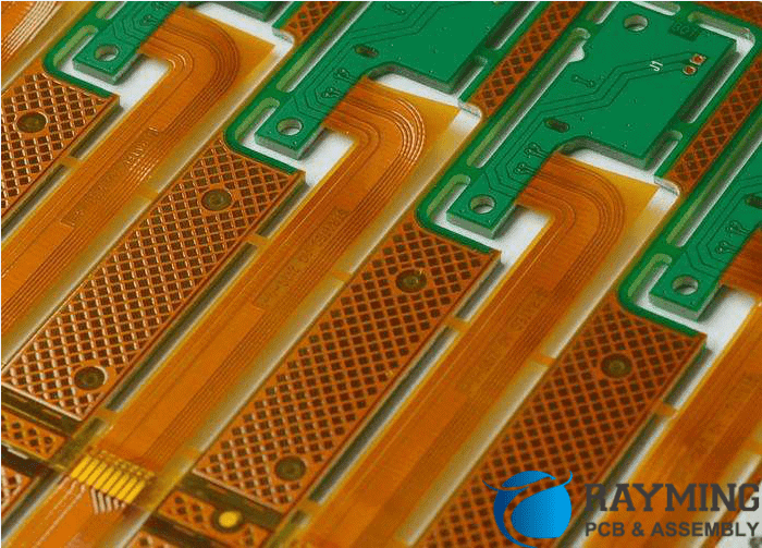
- Challenging for flex PCBs and rigid-flex designs.
Despite difficulties, PCB designers must make every effort to follow the 20H rule for optimal signal integrity. If not feasible, other techniques like shielding, cross-talk mitigation ICs, and differential signaling help alleviate problems.
Example Application of the 20H Rule
Let’s apply the 20H rule to determine trace spacing for a sample scenario:
- 6-layer PCB with signal layers spaced 0.2mm over the ground plane.
- Top layer carries a 5GHz clock signal with 0.2mm track height (H).
- Bottom layer has a 1MHz SPI interface with 0.2mm track height.
For the 5GHz clock:
- H = 0.2mm
- Minimum spacing from 20H rule = 20 * H = 20 * 0.2mm = 4mm
This 4mm spacing must be maintained between clock traces to prevent crosstalk.
For the 1MHz SPI interface:
- H = 0.2mm
- Minimum spacing from 20H rule = 20 * H = 20 * 0.2mm = 4mm
However, this is a low-frequency signal so the 20H rule may be exempted. 1mm spacing would likely suffice if traces are kept away from clock signals.
FAQs
What are some key points to remember about the 20H rule?
- Applies to high-speed traces susceptible to crosstalk.
- Ensures spacing of at least 20 times trace height H above the reference plane.
- Prevents crosstalk, maintains impedance, accommodates return currents.
- Challenging to implement but critical for signal integrity.
- Must be considered during component placement and routing.
Does the 20H rule apply to traces sandwiched between ground planes?
Yes, the reference plane in the 20H rule applies to adjacent ground planes above and below the trace. Sandwiching traces between solid ground planes is an ideal stackup for EMI control. The 20H rule spacing should be followed between traces with this layer configuration as well.
Can the 20H rule be violated if crosstalk is modeled and acceptable?
It is not advisable to violate the 20H rule even if modeling suggests crosstalk is within limits. Electromagnetic coupling changes with varying field strengths, frequencies, edge rates, impedances, and transmission line effects. Models have limitations and assumptions. Violating established spacing rules leaves margin for error and reliability issues.
Are there any alternatives to the 20H rule for dense PCBs?
For dense PCBs where 20H rule would be difficult, other options like differential signaling, crosstalk cancellation ICs, embedded waveguides, shielding ground traces, and orthogonal routing help control crosstalk. These techniques allow slight exemptions from the spacing rule but do not eliminate the need for it altogether.
Does the 20H rule apply to traces passing orthogonally?
Yes, the 20H rule spacing must also be maintained between traces passing orthogonally or at angles. Electric fields couple between perpendicular traces so the spacing requirement remains unless shielding is used at intersection points.


Leave a Reply