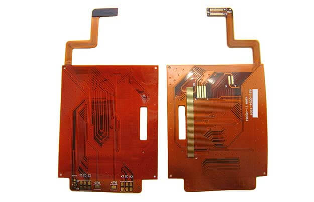
Introduction
Potting is the process of filling the empty spaces on a printed circuit board (PCB) with a protective polymer compound. Potting encapsulates the electronic components and circuitry on the PCB within an insulating material for protection against environmental stresses like moisture, vibration, shock, dust etc.
Some key aspects regarding potting of PCBs:
- Potting inhibits the penetration of moisture and corrosive contaminants into the PCB.
- It provides mechanical support by damping vibration, absorbing shock and preventing flexing damage.
- Potting improves thermal performance by transferring heat away from components.
- It protects PCBs from harsh outdoor environments and even underwater conditions.
- Common potting materials include epoxy, silicone, polyurethane or acrylic compounds.
- Dispensing systems are used to inject measured amounts of potting material onto the PCB.
- selective potting of critical areas helps optimize cost, weight and manufacturability.
Reasons for Potting PCBs
Here are some of the main reasons potting is used for PCBs:
Moisture and Chemical Resistance
- Potting seals out moisture, humidity, condensation, salt spray etc. which can corrode the PCB.
- It prevents contaminants like dust, grease, chemicals etc. from reaching electronics.
Vibration and Shock Resistance
- The cured potting material firmly holds components in place and absorbs shock/vibration.
- Prevents microcracks or fractures in solder joints and traces due to mechanical stresses.
Noise Isolation
- Acoustic noise from high frequency PCBs can be dampened by potting.
- Potting helps reduce electromagnetic interference radiating from the board.
Thermal Dissipation
- Potting improves heat transfer away from hot components into surrounding air.
- Some potting compounds have higher thermal conductivity to act as a heat sink.
Product Safety
- Potting prevents user contact with hazardous high voltages on the PCB.
- It provides electrical insulation up to several kV for safety.
Outdoor/Underwater Use
- Potting enables PCB operation in harsh environments like marine, automotive, aerospace etc.
- Some potting compounds allow PCBs to be operated underwater at high pressure.
Potting Materials for PCBs
Various potting compounds are available for protecting PCBs:
Epoxy
- Most common potting material for PCBs.
- Available as two-part thermoset epoxy resins and hardeners cured at room temperature.
- Offer excellent adhesion, chemical resistance, durability and electrical insulation.
- Can withstand high temperatures of over 120°C depending on type.
- Provide good moisture sealing, vibration resistance and thermal conduction.
- Can be opaque or made clear transparent. Available in different shore hardness.
Silicone
- Based on silicone polymers which are flexible, soft and elastic.
- Better shock absorption, vibration damping and thermal cycling performance than epoxy.
- Maintains protection and adhesion over a wide -60°C to 200°C temperature range.
- Disadvantages are higher cost and worse moisture protection than epoxy.
Polyurethane
- Polyurethane potting compounds offer high toughness and abrasion resistance.
- Typically two-part mixtures which cure at room temperature.
- Provide very good protection against moisture and chemicals.
- Softer formulations provide damping against vibration and shock.
- Upper temperature range limited to 80°C for many polyurethanes.
Acrylic
- Acrylic based potting compounds provide optical clarity for LED applications.
- Easy to apply by pouring and low viscosity allows potting small spaces.
- Resistant against humidity, UV radiation and yellowing.
- Limitations are weaker mechanical strength and higher cost.
Potting Process Steps
Applying potting to a PCB involves these key steps:
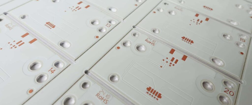
PCB Preparation
- A protective mask is applied on areas of the PCB not to be potted like connectors, testpoints, indicators etc.
- Any internal openings or cavities in the board are sealed to prevent potting leakage.
- Boards are cleaned to remove contaminants and surface mounted devices are glued if needed.
Material Preparation
- Two-part potting compounds are mixed as per specified ratio before applying.
- The working life after mixing is limited based on potting compound used.
- Materials are degassed under vacuum if required to prevent bubbles.
- Dispensing needles and barrels are prepared.
Dispensing
- Potting material is injected onto the PCB using manual or automated dispensing.
- Material is dispensed into openings, along edges and over components in controlled amounts.
- Multiple dispenses may be used to build up thickness and fill in areas.
Curing
- PCBs are left at room temperature or heated ovens for the potting material to cure fully.
- Cure times range from 30 minutes to several hours based on potting compound.
- Excess flash is cleaned from the PCB edges after curing.
Final Testing
- Potted boards undergo thermal, vibration, electrical and functional tests.
- Final quality inspection checks for voids, cracks, coverage uniformity and cosmetic defects.
Potting Equipment
Applying potting materials requires dispensing and curing equipment:
Dispensing Systems
- Manual dispensing uses hand applicators or syringes for small volumes.
- Pneumatic dispensers provide more controlled flow rates and pressurized delivery.
- Automated fluid dispensing robots offer programmable volume control and repeatability.
- Mixing and metering systems produce homogeneous blended two-part compounds.
- Vision alignment, flow sensors and valve controls enable precision automated dispensing.
Curing Ovens
- Simple oven chambers with air circulation are used for heat curing.
- Programmable ovens allow setting timed ramps and soaking as per curing schedule.
- Vacuum degas chambers remove air bubbles prior to applying material.
- Conveyor ovens automate continuous curing for higher throughput.
- UV spot curing systems can selectively cure portions using targeted light.
Design Considerations for Potting
The PCB must be designed with potting in mind:
- Avoid placing tall components near edges which restrict flow into interior areas during dispensing.
- Provide adequate spacing around components for potting material to flow and fill.
- Incorporate dams, trenches and walls to contain material in required zones.
- Include vent holes for air bubbles to escape when potting complex shapes.
- Design enclosures with potting material capacity and injection/overflow points.
- Mark the board with fiducials and boundaries to guide automated dispensing.
- Specify any required electrical insulation thicknesses for voltage isolation.
- Define critical components or sections for selective potting if full-board potting is not needed.
Advantages of Potting PCBs
Key benefits of potting include:
- Greatly increases ruggedness, shock, vibration and flex tolerance.
- Provides excellent protection in moist, dirty or corrosive environments.
- Improves thermal heat dissipation away from components.
- Guards against accidental electrical contact with hazardous voltages.
- Reduces electromagnetic emissions from the board.
- More consistent performance over a wide temperature range.
- Seals out dust, grime and particulate contamination.
- Extends long term reliability with lower failure rates.
Limitations of Potting
Some limitations to consider are:
- Additional materials cost and processing time for potting.
- Potting material adds weight, which may be significant.
- Thermal stresses during curing can affect some components.
- Rework and repairs become difficult or impossible on potted boards.
- De-potting or removing old potting material can be troublesome.
- Potting thicknesses and coverage uniformity is difficult to inspect internally.
- Cured dripping or overflow on connectors, buttons etc. affects aesthetics.
Quality Control
Important aspects to validate quality when potting PCBs:
Potting Material Validation
- Certify each new potting material batch with sample PCBs before use.
- Verify curing, hardness, adhesion, insulation, thermal conductivity etc. by testing.
Process Controls
- Closely follow compound ratios, mix times, degassing and curing schedules.
- Use calibrated dispensing systems and consistent procedures.
Inspection
- Visually inspect for voids, bubbles, oozing over components, coverage uniformity etc.
- X-ray imaging can reveal internal voids and bubbles.
- Confirm thickness measurements using needle probes or cut-away samples.
- Thermal tests verify heat dissipation. Electrical tests validate insulation.
Reliability Testing
- Subject samples to temperature cycling, thermal shock, vibration and drop/shock tests.
- Perform accelerated testing like HAST, ALT and environment chambers.
- Analyze results for any signs of delamination, cracks, electrical leakage etc.
Applications of Potting
Some common applications where potting is used:
Outdoor Equipment
- Weather stations, cameras, sensors etc. exposed to rain, sun, wind and dirt.
Marine Electronics
- Depth finders, fish detectors, navigation devices subject to moisture on boats.
Automotive Electronics
- Engine control units, transmission controllers in hot, humid, vibrating conditions.
Industrial Automation
- PLCs, controllers, sensors in factories with vibration, contaminants.
Aerospace and Aviation
- Airborne systems in thin atmosphere and high vibration conditions.
Medical Devices
- Protecting implanted devices from body environment.
HID Lighting
- High intensity discharge lamps with high voltages up to 5kV.
Conclusion
Potting plays a vital role in protecting PCBs in challenging environments with moisture, vibration, shock, contamination etc. Selecting appropriate potting materials and processes is key to achieving effective and reliable protection. With attention to design to accommodate potting and validating the materials and quality, potted boards can survive much harsher mechanical and ambient conditions. This enables electronics to operate reliably in demanding applications from offshore systems to implanted medical devices.
Frequently Asked Questions
Q1. What materials are used for potting PCBs?
Epoxy is the most common followed by silicone and polyurethane. Materials are selected based on electrical, mechanical, thermal and cost requirements.
Q2. Does potting add a lot of weight to PCBs?
Yes, potting does add significant weight depending on the coverage area and thickness. This needs consideration in design.
Q3. Can connectors and indicators be left unpotted?
Yes, critical areas can be masked off before potting. But seals are needed to prevent material ingression.
Q4. Does potting reduce EMI from PCBs?
Potting material can attenuate EMI emission from the board and shields sensitive circuits from external fields.
Q5. Can potting be removed for rework or repairs?
Potting is very difficult to remove once cured fully. Selective potting only critical areas facilitates repairability.


Leave a Reply