Understanding PCB Visualizer
What is a PCB?
A printed circuit board (PCB) is a fundamental component in modern electronics. It is a flat board made of insulating materials, such as fiberglass or plastic, with conductive tracks, pads, and other features etched onto its surface. PCBs provide a means to mechanically support and electrically connect electronic components using conductive pathways, tracks, or signal traces.
The Role of PCB Visualizer
PCB Visualizer plays a crucial role in the PCB design process by providing a visual representation of the circuit board layout. It allows users to:
- Create schematic diagrams
- Design the physical layout of the PCB
- Place and route components
- Perform design rule checks (DRC)
- Generate manufacturing files
By using PCB Visualizer, designers can ensure that their PCB designs are accurate, efficient, and compliant with industry standards and manufacturing requirements.
Key Features of PCB Visualizer
Schematic Capture
PCB Visualizer provides a schematic capture feature that allows users to create electronic Circuit Diagrams. The schematic capture tool includes:
- A library of electronic components
- Support for hierarchical designs
- Electrical rule checking (ERC)
- Netlist generation
PCB Layout Design
Once the schematic is complete, PCB Visualizer enables users to create the physical layout of the PCB. The PCB layout design features include:
- Automatic and manual component placement
- Routing tools for creating conductive tracks
- Support for multi-layer boards
- Design rule checking (DRC) to ensure manufacturability
3D Visualization
PCB Visualizer offers 3D visualization capabilities, allowing users to view their PCB designs in a three-dimensional space. This feature helps in:
- Identifying potential mechanical interferences
- Verifying component placement and clearances
- Generating realistic renderings for presentations and documentation
Collaboration and Version Control
PCB Visualizer supports collaboration and version control features, enabling teams to work together efficiently on complex PCB projects. These features include:
- Real-time collaboration and design sharing
- Revision history and version control
- Design merging and conflict resolution

Benefits of Using PCB Visualizer
Improved Design Efficiency
PCB Visualizer streamlines the PCB design process, reducing the time and effort required to create high-quality PCB layouts. Its intuitive interface and automated features, such as auto-routing and design rule checking, help designers work more efficiently and avoid common design errors.
Enhanced Design Quality
By providing a comprehensive set of design tools and real-time feedback, PCB Visualizer helps designers create PCBs that are optimized for performance, reliability, and manufacturability. The software’s design rule checking capabilities ensure that the PCB layout adheres to industry standards and manufacturing constraints, minimizing the risk of production issues and delays.
Collaborative Design Process
PCB Visualizer’s collaboration features enable team members to work together seamlessly, regardless of their location. Real-time design sharing and version control capabilities allow multiple designers to contribute to a project simultaneously, improving communication and reducing the risk of errors and inconsistencies.
Cost Savings
Using PCB Visualizer can lead to significant cost savings in the PCB design and manufacturing process. By catching design errors early and ensuring compliance with manufacturing requirements, designers can avoid costly redesigns and production delays. Additionally, the software’s optimization features help minimize material usage and improve manufacturing efficiency, reducing overall production costs.

Getting Started with PCB Visualizer
System Requirements
Before installing PCB Visualizer, ensure that your computer meets the following minimum system requirements:
| Component | Minimum Requirement |
|---|---|
| Operating System | Windows 7, 8, 10, or 11 |
| Processor | Intel Core i5 or equivalent |
| RAM | 8 GB |
| Display Resolution | 1920 x 1080 |
| Graphics Card | Direct3D 11 |
Installation Process
To install PCB Visualizer, follow these steps:
- Download the PCB Visualizer installer from the official website.
- Run the installer and follow the on-screen instructions.
- Accept the license agreement and choose the installation directory.
- Select the components you want to install (e.g., libraries, templates).
- Wait for the installation process to complete.
- Launch PCB Visualizer from the desktop shortcut or the Start menu.
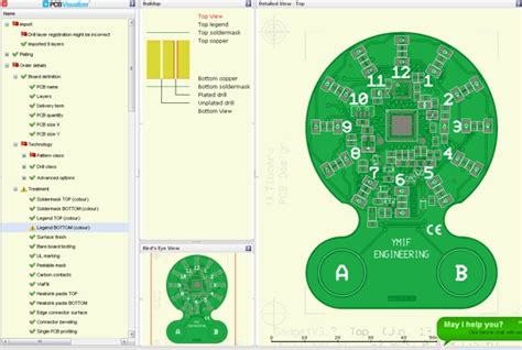
User Interface Overview
PCB Visualizer’s user interface is designed to be intuitive and user-friendly. The main window consists of the following areas:
- Menu bar: Provides access to various tools, settings, and file management options.
- Toolbar: Contains frequently used tools and commands for quick access.
- Workspace: Displays the schematic diagram or PCB layout, depending on the active view.
- Component library: Shows available electronic components and allows searching and filtering.
- Properties panel: Displays and allows editing of the properties of selected objects.
- Output panel: Provides feedback, warnings, and error messages during the design process.

PCB Design Workflow
Creating a New Project
To start a new PCB design project in PCB Visualizer, follow these steps:
- Click on “File” in the menu bar and select “New Project.”
- Choose a project template or start with a blank project.
- Specify the project name, location, and other relevant settings.
- Click “Create” to initialize the new project.
Schematic Capture
The schematic capture process involves creating a graphical representation of the electronic circuit. To create a schematic in PCB Visualizer:
- Open the schematic editor by double-clicking on the schematic file in the project tree.
- Drag and drop components from the library onto the schematic canvas.
- Connect the components using wires or nets.
- Assign component values, footprints, and other properties as needed.
- Perform electrical rule checks (ERC) to verify the schematic’s integrity.
PCB Layout Design
Once the schematic is complete, you can proceed to the PCB layout design phase. To create a PCB layout in PCB Visualizer:
- Open the PCB layout editor by double-clicking on the PCB File in the project tree.
- Define the board outline and any mechanical constraints.
- Place components on the board, either manually or using automatic placement tools.
- Route the connections between components using the available routing tools.
- Define copper pour areas, vias, and other PCB features as needed.
- Perform design rule checks (DRC) to ensure the layout’s manufacturability.
Generating Manufacturing Files
After completing the PCB layout, you can generate the necessary manufacturing files. PCB Visualizer supports various output formats, including:
- Gerber files: Industry-standard format for PCB fabrication.
- Drill files: Specifies the location and size of drill holes on the PCB.
- Bill of Materials (BOM): Lists all components used in the design.
- Assembly drawings: Provides visual guidance for PCB Assembly.
To generate manufacturing files in PCB Visualizer:
- Click on “File” in the menu bar and select “Fabrication Outputs.”
- Choose the desired output formats and settings.
- Specify the output directory and file names.
- Click “Generate” to create the manufacturing files.
Advanced Features and Techniques
Multi-Layer PCB Design
PCB Visualizer supports the design of multi-layer PCBs, which are essential for complex and high-density circuits. To create a multi-layer PCB:
- Define the layer stack-up in the PCB properties.
- Assign components and traces to specific layers.
- Use vias to connect traces between layers.
- Ensure proper layer alignment and clearances.
High-Speed Design Considerations
When designing PCBs for high-speed applications, such as high-frequency digital circuits or radio frequency (RF) devices, special considerations must be taken. PCB Visualizer offers features to address high-speed design challenges, including:
- Controlled impedance routing
- Differential pair routing
- Length matching and delay tuning
- Signal integrity analysis
To utilize these features, consult the PCB Visualizer documentation and apply best practices for high-speed PCB design.
Design Reuse and Libraries
PCB Visualizer allows you to create and manage libraries of reusable components, footprints, and design blocks. By utilizing libraries, you can save time and ensure consistency across multiple projects. To create and use libraries:
- Create a new library or open an existing one.
- Add components, footprints, or design blocks to the library.
- Assign properties and parameters to the library elements.
- Save the library and use it in future projects.
Frequently Asked Questions (FAQ)
- What file formats does PCB Visualizer support?
PCB Visualizer supports various industry-standard file formats, including: - Schematic: KiCad, Eagle, Altium Designer, and more
- PCB Layout: Gerber, ODB++, IPC-2581, and more
- Can PCB Visualizer import designs from other software?
Yes, PCB Visualizer can import designs from other popular PCB design software, such as KiCad, Eagle, and Altium Designer. Simply use the “File” > “Import” option and select the appropriate file format. - How does PCB Visualizer handle design rule checks (DRC)?
PCB Visualizer includes a comprehensive set of design rule checks to ensure the manufacturability and reliability of your PCB designs. You can configure the DRC rules based on your specific requirements and run the checks at any time during the design process. The software will highlight any violations and provide guidance on how to resolve them. - Can multiple users collaborate on a PCB design in PCB Visualizer?
Yes, PCB Visualizer supports real-time collaboration and version control features. Multiple users can work on the same project simultaneously, with changes synced in real-time. The software also tracks revisions and allows for design merging and conflict resolution. - Is PCB Visualizer suitable for beginners?
While PCB Visualizer is a powerful and feature-rich tool, it is designed to be user-friendly and accessible to users of all skill levels. The software includes extensive documentation, tutorials, and a helpful community forum to assist beginners in getting started with PCB design. Additionally, PCB Visualizer offers a variety of templates and wizards to guide users through common design tasks.
Conclusion
PCB Visualizer is a comprehensive and user-friendly tool that streamlines the PCB design process, from schematic capture to manufacturing file generation. Its powerful features, including 3D visualization, design rule checking, and collaboration capabilities, make it an essential tool for engineers, designers, and enthusiasts alike.
By following the guidelines and best practices outlined in this article, you can leverage PCB Visualizer to create high-quality, reliable, and manufacturable PCB designs. Whether you are a beginner or an experienced designer, PCB Visualizer provides the tools and flexibility needed to bring your electronic projects to life.


Leave a Reply