Introduction to PCB Etching
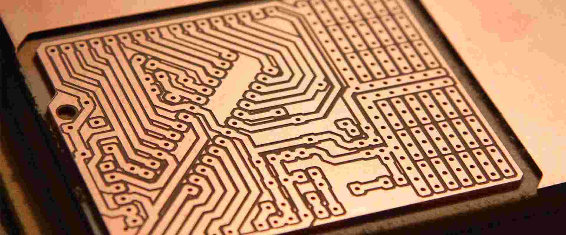
Printed circuit board (PCB) fabrication involves multiple processes that transform the electrical circuit board design into a physical board. One of the most critical steps is PCB etching.
Etching forms the conductive copper traces on the PCB that provide the electrical connections between components. The etching process selectively removes unwanted copper from the copper-clad laminate to leave only the desired conductive pattern defined by the circuit layout.
Understanding PCB etching helps designers optimize designs for manufacturability and select appropriate fabrication processes. This article provides an in-depth overview of etching for PCB production.
Role of Etching in PCB Fabrication
PCB fabrication can be summarized in three main stages:
- Imaging – Transfer the conductor pattern onto the copper foil.
- Etching – Remove unwanted copper to leave only intended conductors.
- Plating – Coat conductors with solder mask and final plating finishes.
Etching is the critical step that physically forms the traces and pads that carry signals, power, and ground. The sequence is:
- Copper-clad laminate sheet with continuous copper foil.
- Photoresist coating and imaging to form a mask.
- Etching to remove exposed copper, leaving only desired conductors.
- Strip photoresist mask after etching completed.
This article focuses on detailing the inner workings of the etching process and methods.
How Does PCB Etching Work?
PCB etching involves controlled chemical dissolution of copper atoms from the areas to be removed. The general etching mechanism is:
- Clean – The copper surface is cleaned to remove oils and oxide.
- React – Etchant solution reacts with exposed copper atoms. An oxidation-reduction reaction occurs.
- Dissolve – The etched copper ions dissolve into the solution as salts.
- Flush – Etching byproducts are flushed away by solution flow. Fresh etchant continues reacting with copper.
The key is localizing the etching only on exposed regions by using a photoresist mask. This leaves conductors protected by resist intact.
Different etching methods use various chemical reactions to oxidize and dissolve the copper atoms. Let’s examine the popular methods.
Types of Etching Processes
There are three predominant PCB etching processes used in fabrication:
Wet Chemical Etching
- Oldest etching technique, uses liquid etchant bath
- Most common method for prototype and small volume production
- Isotropic etching (etches evenly in all directions)
- Lower cost equipment but slower and less precise
Dry Etching
- Uses gaseous plasma to etch copper
- Anisotropic etching (etches directionally)
- More expensive equipment but faster and capable of finer features
- Used for HDI boards requiring tight tolerances
Laser Etching
- Directs high power laser beam to ablate copper
- Extremely precise with no mask required
- Ideal for rapid prototyping of design changes
- Limited by lower throughput and higher cost
Next we’ll examine each of these PCB etching methods and their relative pros and cons in more detail.
Wet Chemical Etching Process
Wet chemical etching has been used since the earliest days of printed circuits. It offers a simple and inexpensive etching technique.
The key steps in the wet etching process are:
- Clean – The copper-clad laminate board is thoroughly cleaned.
- Coat – Photoresist is applied to the copper layers.
- Expose – The resist is exposed to UV through the mask.
- Develop – Photoresist is developed, hardening exposed regions.
- Etch – The board is immersed in etching solution, dissolving exposed copper.
- Strip – Remaining resist is stripped away after etching completes.
Etchant Chemicals
Common chemical etchants used for copper include:
- Ferric Chloride (FeCl3) – Most popular and cost-effective etchant.
- Ammonium Persulfate ((NH4)2S2O8) – More eco-friendly but inferior etch quality.
- Cupric Chloride (CuCl2) – Isotropic etchant with high copper solubility.
Wet etchants are sold in liquid concentrate form and mixed with water at the specified dilution ratios. The chemicals oxidize and dissolve exposed copper regions.
Etching Mechanism
The wet etching process involves reduction of Cu atoms into Cu2+ ions which enter the solution:
- Anodic reaction: Cu -> Cu2+ + 2e-
- Cathodic reaction: Fe3+ + e- -> Fe2+
- Overall redox: 2Fe3+ + Cu -> 2Fe2+ + Cu2+
Ferric chloride is regenerated allowing continuous etching until solution is fully saturated with copper ions.
Etch Profile
Since wet etching is isotropic, it etches in all directions at approximately the same rate:
- Lateral etching undercuts the conductors, limiting precision
- Etch rates range from 25-100 μm/min depending on concentrations
Dry Etching Process
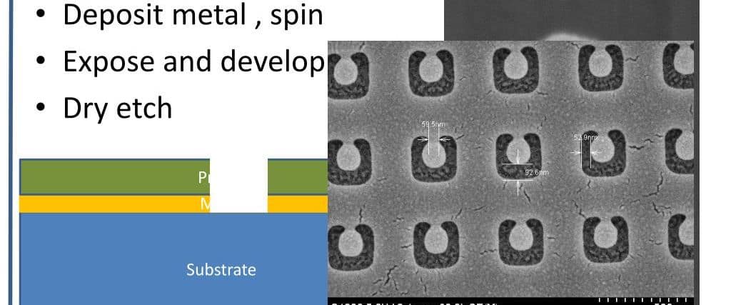
Dry etching uses gas plasma technology to etch copper instead of liquid chemicals. The main steps are:
- Coat – Photoresist is applied and imaging performed.
- Expose – Board is exposed to plasma containing reactive gases.
- React – Ions dissociate and react with exposed copper regions.
- Volatilize – Etch byproducts are volatile gases and evacuate chamber.
- Strip – Remaining resist mask is chemically stripped away.
Plasma Sources
PCB dry etching systems typically use either:
- Glow discharge plasma
- Reactive ion etching plasma
Radio frequency electromagnetic fields ionize the low-pressure gas mixture inside a vacuum chamber.
Reactive Gases
Common gases used in PCB copper etching include:
- Oxygen – Most common to oxidize copper
- Chlorine – Highly reactive but more hazardous
- Sulfur Hexafluoride – Can yield anisotropic profiles
The reactive ions bombard and oxidize exposed copper regions on the PCB.
Etch Profile
Dry etching produces an anisotropic etch profile:
- Etches predominantly downward with minimal undercut
- Allows finer resolution down 3-5 μm range
- Etch rates up to 100 μm/min
The directional etch allows tighter tolerances for dense interconnects on advanced PCBs.
Laser Etching Process
Laser etching uses a focused high power laser beam to precisely ablate copper surfaces:
Laser Types
- CO2 lasers – Most common; 10.6 μm wavelength
- Nd:YAG lasers – Can produce finer resolution
- Fiber lasers – High precision with stable output
Laser Parameters
- Power density ~105 W/cm2
- Pulsing modes – Continuous wave, burst, or single shot
- Scan speed – Up to 500 mm/s
Etching Mechanism
Laser etching vaporizes copper through intense localized heating:
- Photons are absorbed by copper surface
- Energy heats copper above boiling point
- Copper vaporizes at temperatures above 2500°C
No mask required – laser is software programmed for the required pattern.
Etch Quality
Advantages of laser etching:
- Extremely fine etch resolution down to 12 μm
- No chemicals required
- Minimal undercut for precise conductors
- Can etch through coatings like ENIG
Laser etching excels at rapid turnaround of prototyping design iterations.
Photoresist Etching Process Comparison
| Process | Photoresist | Etchant | Etch Profile | Resolution | Speed | Cost |
|---|---|---|---|---|---|---|
| Wet | Liquid | Chemical bath | Isotropic | Low | Slow | Low |
| Dry | Liquid | Gas plasma | Anisotropic | High | Fast | High |
| Laser | None | Laser beam | Anisotropic | Highest | Fastest | High |
In summary, wet etching is the cost-effective process for small to mid-volume production while dry etching and laser excel for high density interconnect (HDI) boards requiring precision.
Optimizing PCB Layouts for Etching
Several layout design guidelines help optimize manufacturability for the etching process:
Trace Width
- Minimum width is a function of etch resolution
- Increase widths on outer layers more prone to overetching
- Size wide traces for controlled impedance where needed
Clearances
- Observe minimum clearance rules between adjacent traces
- Account for undercut to prevent shorts – add clearance for wet etching
Anchor Pads
- Use anchor pads on traces ending at vias or pads
- Prevents undercut from detaching thin traces
Dense Areas
- Watch for inadequate clearance in dense interconnect areas
- May require design changes or HDI stackup
Balance Copper
- Equalize copper densities across layers
- Reduces risk of etchant starving dense regions
Design Margins
- Apply guard bands and margins to compensate for tolerances
- Allows for over/under-etch without creating defects
Early engagement with fabrication partners helps assess manufacturability as layouts progress.
PCB Etching Defects
Several common PCB etching defects can impact yield. Understanding causes aids prevention through design and process adjustments.
Overetching
Overetching removes excessive copper, compromising conductor thickness and widths. Causes include:
- Excessive etch cycles or duration
- High etchant temperature increases reaction rate
- Low copper density areas etch faster
Underetching
Underetching leaves unwanted copper residues causing potential shorts. Contributing factors are:
- Insufficient etchant solution flow
- Depleted etchant solution with reduced reactivity
- Insufficient etching time for the copper thickness
Overhang Etching
Overhang etching induces excessive lateral undercut of traces under the resist edge. Factors include:
- Using solder mask instead of permanent resist
- Prolonged etching duration
- Highly isotropic etch process
Pitting and Pinholes
Pits and voids in copper surface. Potential sources:
- Contaminated etchant bath
- Poor copper surface prep leaving residues
- Etchant reaction byproducts accumulate
Mask Undercut
Lateral etching under the resist mask leads to loss of fine features. Caused by:
- Old or defective photoresist
- Photoresist process problems causing inadequate hardening
- Etchant seeping under the mask edge
Improving Etch Quality and Consistency
Several best practices help optimize etch quality and minimize defects:
- Maintain proper chemical concentrations in etchant bath
- Use filtration to remove contaminants and particulates
- Agitate etchant solution to ensure uniform access
- Closely control etchant temperature for repeatability
- Regularly regenerate chemical baths as they degrade
- Rinse boards thoroughly after etching to halt reactions
- Standardize photoresist application, exposure and development
- Institute regular coil etching process audits
- Test etch rates periodically using coupons
Adhering to disciplined procedures reduces variability and drives consistent high quality etching.
Environmental Considerations for Etching
The bulk chemicals used in PCB etching have environmental health and safety considerations:
- Ferric chloride is corrosive and a mild irritant
- Ammonium persulfate is an irritant and sensitizer
- Cupric chloride is very toxic to aquatic life
Best practices for responsible etching include:
- Use minimum required chemical concentrations
- Operate baths at optimum temperatures – not excessive
- Store chemicals properly in sealed containers
- Neutralize etchant waste before disposal
- Recover copper from spent etchant if economical
- Partner with chemical disposal firms to properly handle waste
- Implement controls to prevent releases or spills
- Provide suitable PPE protection for workers
While essential to PCB production, etching does require careful environmental management.
The Future of PCB Etching
PCB etching technology continues advancing to meet the needs of electronics innovation:
Dry Etching Growth
- Dry etching expands further as HDI designs become mainstream – offers superior precision
Multi-Chemistry Etching
- Using different etching steps tailored for specific board layers allows optimizing each step.
Laser Etching Improvements
- Faster scan speeds and lower costs make laser etching viable for higher volume production.
Reduced Chemistry Etching
- Lower chemistry etching techniques help minimize chemical waste and hazards.
Digital Etching
- Digital imaging eliminates need for physical masks and allows rapid design changes.
Etchant Recycling
- Recycling etching chemicals from spent baths reduces waste.
Smarter etching processes will continue enabling PCB technology to progress and support electronics advancement.
Conclusion
Etching is the defining fabrication step that physically forms the conductive pattern on printed circuit boards. While evolving from early dangerous acid etching, modern PCB etching still relies heavily on chemicals. Understanding the principles, mechanisms, equipment, limitations, and environmental factors is key to effective design and process engineering.
Continued etching innovation will provide solutions balancing precision, speed, cost, and sustainability – enabling further progress in PCBs and electronics.
Etching FAQs
What are the main advantages of dry etching over traditional wet etching?
Dry etching offers much finer resolution down to around 5 μm due to its anisotropic etch profile. It also enables much higher etch rates over 100 μm/min vs 25-100 μm/min for wet.
What effects can overetching have on a PCB?
Overetching reduces the thickness of copper traces which increases electrical resistance and susceptibility to damage. It can also overly narrow trace widths reducing current capacity. Excessive overetching can completely undermine traces.
How does etchant solution agitation improve etching consistency?
Agitation ensures fresh etchant is continuously brought into contact with the copper surface being etched. Stagnant solution can become saturated with copper ions which slows etch rate.
Why is anchor pad design important for wet etching?
Anchor pads help prevent undercut etching from completely detaching thin traces from pads or vias. The enlarged anchor region provides more copper volume to counter undercutting action.
What is the main advantage of laser etching compared to traditional methods?
Laser etching does not require physical masks for imaging. The pattern is programmed directly and ablates copper rapidly. This allows instant design changes without any mask revisions.


Leave a Reply