Introduction
Fiducials are essential features used in printed circuit boards (PCBs) to aid in accurate alignment and assembly. Also referred to as alignment marks or registration marks, fiducials provide fixed reference points that manufacturing machines and assembly equipment use for precise positioning.
Understanding fiducials and their role in the PCB fabrication and assembly process is important for electrical engineers and PCB designers. This article will provide an in-depth look at what fiducials are, the different types used, their functions, and key design considerations when using them.
What is a Fiducial?
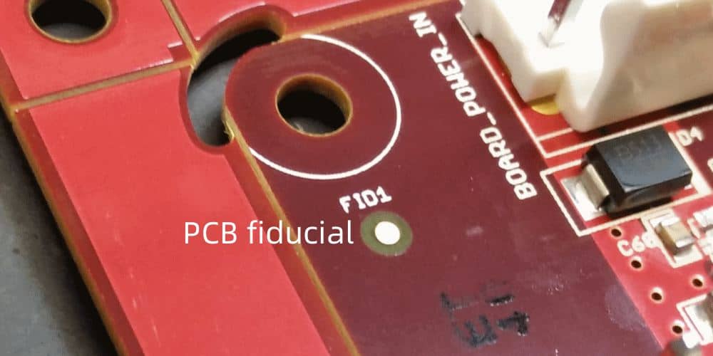
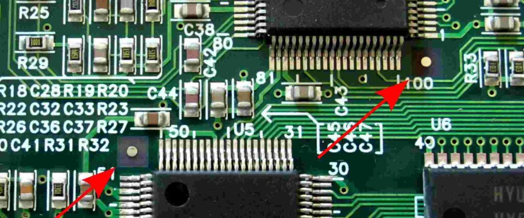
A fiducial is a precisely located marking or target on a PCB that serves as a point of reference for alignment and measurement. Fiducials come in a variety of shapes and sizes, but circular pads or crosses are most common.
On a bare PCB, fiducials stand out clearly from the surrounding copper and substrate to be easily recognized by automated optical inspection systems. The machines locate the fiducial targets and use them to orient and align the board or panel for different fabrication steps.
Fiducials placed on the assembly layers also facilitate component placement equipment locating the board and precisely positioning parts during population. They serve a vital role from fabrication through final assembly.
Key Characteristics
Here are some typical characteristics of PCB fiducials:
- Provide fixed, precise reference locations distributed across the board.
- Clearly visible from copper background with high contrast.
- Allow very accurate measurements from their center or axis.
- Optimized for easy recognition by machine vision systems.
- Remain visible after most PCB processing steps.
- Does not interfere with routing or electrical functionality.
Fabrication Alignment
During PCB fabrication, fiducials provide alignment for processes like:
- Photolithography – Aligning layers to drill holes, vias, etc.
- Registration of solder mask openings.
- Ensuring layers are stacked properly.
- Alignment for routing and scoring PCB panels.
- Panelization of arrays of boards.
Assembly Alignment
Fiducials on assembly layers help align:
- Pick and place machines positioning components.
- Screen printers applying solder paste.
- Automated optical inspection (AOI) equipment.
- Conformal coating systems targeting protective material.
- Flying probe testers checking boards.
- Box build and other post-PCB assembly alignment.
Types of PCB Fiducials
There are a variety of fiducial shapes, sizes, and styles used on PCBs. Here are the most common options:
Copper Pads
- Simple copper pads make ideal fiducials.
- Easy to implement directly in PCB layout.
- Various diameter options from 0.020″ to 0.1″
- Pad fiducials most frequently used for fabrication alignment.
Copper Crosses or X
- Cross shape stands out distinctly from plane layers.
- Compatible with most optical recognition systems.
- Different line widths and sizes available.
- Allows precise positioning at crosshair center.
Drilled Holes
- Holes extending through substrate act as clear fiducials.
- Well-suited for double-sided boards without through-hole components.
- Provides alignment at hole center axis.
- Hole diameter typically 0.02″ to 0.03″.
Non-Copper Targets
- Ceramic-based marks screened onto PCB surface.
- Compatible with solder mask over bare copper designs.
- Withstands high temps and processing chemicals.
- Specialized application, not as widely used.
Text Fiducials
- Symbols, numbers, or letters on silkscreen layer.
- Easily distinguished from bare substrate.
- Primarily used by assemblers for orienting boards.
- Positioning precision not as good as targets.
Key Fiducial Functions and Usage
Fiducials serve some vital functions through the PCB production and assembly workflows. Here are some of the key ways fiducials are utilized:
Layer-to-Layer Registration
Fiducials distributed around the board provide alignment points when registering layers during the imaging process. This ensures features on different layers are properly stacked in relation to each other. Registration can detect and compensate for any image layer shifts.
Phototool to Panel Registration
Panelization systems use fiducials to precisely align multiple PCB images on a phototool mask to the panels being exposed. This achieves accurate registration of each board outline to the routed panel edges.
Solder Mask Alignment
Opening in the solder mask layer are aligned to the underlying features using the fiducials as anchors. This prevents mask openings from being misaligned over pads and traces.
Panelizing Boards
Fiducials on individual boards assist the panelization router in accurately spacing and aligning boards when cutting panel sections.
Assembly Machines
Pick-and-place, screen printers, AOI systems, and other assembly equipment align to fiducials to locate the ideal component placement positions.
Post-Assembly Processes
Steps like conformal coating jets target fiducial locations to properly coat boards. Flying probe testers also use fiducials for board alignment.
Locating Fiducials on a PCB
To maximize effectiveness, fiducials must be intelligently positioned. Here are guidelines on fiducial placement:
- Include at least 2 fiducials, often more for larger boards. 3-6 commonly used.
- Place near opposite corners of board for orientation.
- Locate fiducials along critical edges or function groupings.
- Keep away from edges that may be skewed during routing.
- Allow 1.5x to 2x fiducial diameter spacing from other features.
- Place similar X/Y distance from center of board for symmetry.
- Include extra fiducials on panel frames for panelization.
Fiducial Design Rules and Settings
Certain design rules should be followed when laying out fiducials in your PCB design software. Here are typical settings:
Copper Pad Fiducials
- Diameter: 0.040″ to 0.10″
- Pad shape: Round
- Hole diameter: None
- Drill span: NA
- Keepout: 1.5x to 2x fid. diameter
Copper Cross Fiducials
- Size: 0.08″ to 0.15″
- Line width: 0.010″
- Layer: Usually on inner layer
- Drill span: NA
- Keepout: 1.5x fid. length
Drilled Hole Fiducials
- Hole diameter: 0.020″ to 0.030″
- Pad diameter: 0.060″ to 0.10″
- Drill span: Same as hole size
- Keepout: 1.5x drill span
Fabricating Fiducials
There are some special fabrication considerations for different fiducial types:
Copper Pads
No special treatment needed. Pads are standard copper features etched like other conductors. Often placed on inner layers.
Copper Crosses
Mostly standard fabrication. Ensure fiducial conductor lines have sufficient width to fully transfer during plating.
Drilled Holes
Fiducial holes are drilled to match their callout diameter after imaging. Plated through or unplated options.
Non-Copper
Require screen printing ceramic-polymer material in fiducial pattern. Withstands processing. Added after most fabrication steps.
Fiducial Recognition and Inspection
Automated inspection systems are critical for utilizing fiducials. Here is an overview:
- Use computer vision and pattern matching to identify fiducial shape.
- Checks for presence and acceptable condition of fiducials.
- Confirms registration distance between fiducials matches design.
- Inspects for any obstructing defects over fiducial area.
- Measures coordinate offsets to fiducial center point very precisely.
- Detects fiducial translation, rotation, and scaling.
Key Fiducial Inspection Tests
Fiducials undergo rigorous automated optical inspection including:
- Presence – Verify fiducial is physically present and detectable.
- Acceptability – Check fiducial meets minimum size and quality criteria.
- Registration – Confirm measured spacing between fiducials matches design.
- Obstruction – Fiducial area is free of any blocking defects.
- Accuracy – Deviation from expected center point or axis position.
- Contrast – Adequate difference from background to be optically detected.
Fiducial Inspection Standards
Machine vision inspection of fiducials must meet precision standards, including:
- <ins>Acceptability Criteria</ins>
- Fiducial fully transferred and discernable
- Edges clear and free of nicks/cracks
- Meets minimum defined size requirement
- <ins>Accuracy Tolerances</ins>
- Offset from taught fiducial center < 0.001″
- Fiducial registration error < 0.003″
- Allowable expansion/contraction < 0.5%
- <ins>Detection Repeatability</ins>
- Position deviation < 0.0005″
- 99.9% valid detection rate over 500 inspections
Fiducial Usage in Assembly
Fiducials provide vital alignment functions during PCB assembly.
Pick-and-Place Machines
- Uses fiducials to locate board position and rotation.
- References component placement to the fiducials.
- Confirms positional accuracy by verifying fiducial locations.
Solder Paste Printers
- Align stencils and boards based on fiducials before print.
- Optically confirm fiducial positions match expected.
- Some printers actively adjust for stretch and offset errors.
AOI Inspection
- Checks assembly quality and component positions relative to the fiducials.
- Detects any placement accuracy errors or skew.
- Verifies conformal coating alignment using fiducials.
Fiducial Design Considerations
Here are some key points for engineers to consider when designing in fiducials:
- Include at least 2 fiducials, but often more needed for large or complex boards.
- Position fiducials away from board edges susceptible to routing deviations.
- Add fiducials on unused areas of boards if space allows.
- Keep clearance area around fiducials free of other features.
- For double-sided boards, add fiducials on both sides.
- Place fiducials symmetrically relative to board center area.
- Consider adding extra fiducials on panel frames.
- Use dedicated fiducial layers in designs if permitted.
Fiducial Problems to Avoid
Some potential issues related to fiducials that should be prevented:
- Insufficient number – Adding too few fiducials can compromise alignment capability.
- Placement too close to edges – Edges can become skewed leading to fiducial shift.
- Near high heat components – Excess heat can compromise fiducial visibility.
- Lack of symmetry – Poorly balanced fiducial placement reduces precision.
- Inadequate clearance – Other features too close to fiducial disrupts detection.
- Incorrect layer – Fabricating on a bottom layer obscures them for assembly.
- Not on panel frames – Limits the ability to align panels.
- Inconsistent design rules – Varying fiducial properties between boards makes automation harder.
Frequently Asked Questions
What are the most commonly used fiducial sizes?
For copper pad fiducials, sizes from 0.040″ to 0.100″ diameter are typical. 0.075″ is a widely used standard size. For copper crosses, 0.10″ to 0.15″ length is common.
Where is the best location to place fiducials on a PCB?
Near the corners of the board about halfway along the edges. Having one fiducial in each board quadrant provides good symmetry and coverage.
Should fiducials be placed on internal board layers?
Fiducials are often located on internal layers since they may be obscured by components if placed on outer layers. This allows them to remain usable throughout the PCB fabrication process.
How are fiducials created on a PCB?
Copper pad fiducials are standard copper features on inner layers. Copper crosses require line draw elements. Drilled hole fiducials need corresponding pad and drill span settings. Non-copper fiducials require specialty screen printing.
Should fiducials be covered by solder mask?
It is generally recommended to leave fiducials uncovered by solder mask whenever possible. This provides the best optical contrast. If covered, transparent mask over fiducials is preferred.


Leave a Reply