Introduction to PCB stencils
A PCB stencil is a thin metal sheet that is used to apply solder paste onto a printed circuit board (PCB) during the surface mount assembly process. The stencil has cutouts that match the pad layout on the PCB, allowing solder paste to be squeezed through onto the pads where components will be placed.
Using a stencil is a fast and accurate way to deposit the correct amount of solder paste – the sticky mixture of solder particles and flux – onto a board before surface mount components are assembled. This ensures good solder joints and reliable connections between components and the PCB after reflow soldering.
PCB stencils are a critical part of the surface mount technology (SMT) assembly process and enable high volume production of circuit boards with repeatable, high quality results. This article provides an in-depth look at what PCB stencils are, how they work, types of stencils, and other key information related to stencil design, materials, usage, and maintenance.
What is the role of a PCB stencil?
A PCB stencil serves several important functions in SMT assembly:
- Accurately deposits solder paste – The stencil cutouts and thickness are designed to transfer the right amount of solder paste to match the pads on the PCB. This prevents problems like insufficient solder and bridging between pads.
- Speeds up solder paste application – A stencil allows solder paste to be rapidly and evenly applied across an entire board rather than manually printing individual pads.
- Enables processing of fine pitch components – Stencils allow very accurate solder paste printing even for tiny chip components with fine pitch between pads.
- Improves repeatability and consistency – Using a stencil results in less variation in solder paste deposits versus manual application. This supports high volume production.
- Reduces solder paste waste – With manual solder paste dispensing, a large proportion ends up wasted. Stencil printing transfers most of the paste to the PCB.
- Facilitates assembly automation – Stencil printing works seamlessly with pick and place machines for automated assembly.
In summary, a PCB stencil is integral to high-speed, high-quality, repeatable surface mount assembly especially for complex, densely populated boards. It deposits the right amount of solder paste where it is needed to assemble components efficiently.
How does a PCB stencil work?
A PCB stencil works through a very simple mechanism during the solder paste printing process:
- The stencil is aligned over the PCB so the stencil openings match the pad layout.
- Solder paste is applied evenly across the top surface of the stencil, usually by rolling over it with a squeegee.
- The solder paste fills the stencil openings and makes contact with the PCB pads below.
- The stencil is then carefully lifted off, leaving precise solder paste deposits on the pads.
- Components are then placed onto the solder paste using pick-and-place machines.
- The PCB goes through a reflow oven, melting the solder paste to form solder joints.
The effectiveness of the process depends on the stencil being an accurate 1:1 representation of the PCB pad layout, with the correct aperture sizes. The thickness and material also impacts how well paste releases. Proper alignment and setup is also key for optimum transfer efficiency.
What are the key specifications and features of a PCB stencil?
PCB stencils have certain key characteristics and parameters that determine their performance and usage:
| Specification | Description |
|---|---|
| Dimensions | Stencil frame dimensions match the PCB outer dimensions. The stencil apertures match the pad geometries. |
| Thickness | Typical thicknesses are 2-8 mils. Thicker stencils deposit more paste but may not release well. Thinner stencils reduce bridging but deposit less paste. |
| Tolerances | Cutouts are precision machined to tight tolerances of +/- 5 microns. Tighter tolerances improve accuracy. |
| Materials | Stainless steel is most common. Nickel plated, brass or polymers are also options. Material affects strength, durability and paste release. |
| Surface finish | Electropolish, laser cut or chemical etch finishes ensure dimensional accuracy. Nanocoatings can be applied to enhance paste release. |
| Support features | Support tabs prevent large apertures from falling out. Countersinks provide clearance for tall components. Marks aid alignment. |
| Frame types | Common frames include rectangular, universal, adjustable and proprietary quick release frames to hold the stencil foil. |
| Other features | Cleaning ports, edge bead compensation, and glue dots help optimize the stencil printing process. |
Choosing the right stencil specifications and features is important to get good paste transfer yield, reduce defects, and enable high volume production.
What are the different types of PCB stencils?
There are several types of PCB stencils designed for different applications and production environments:
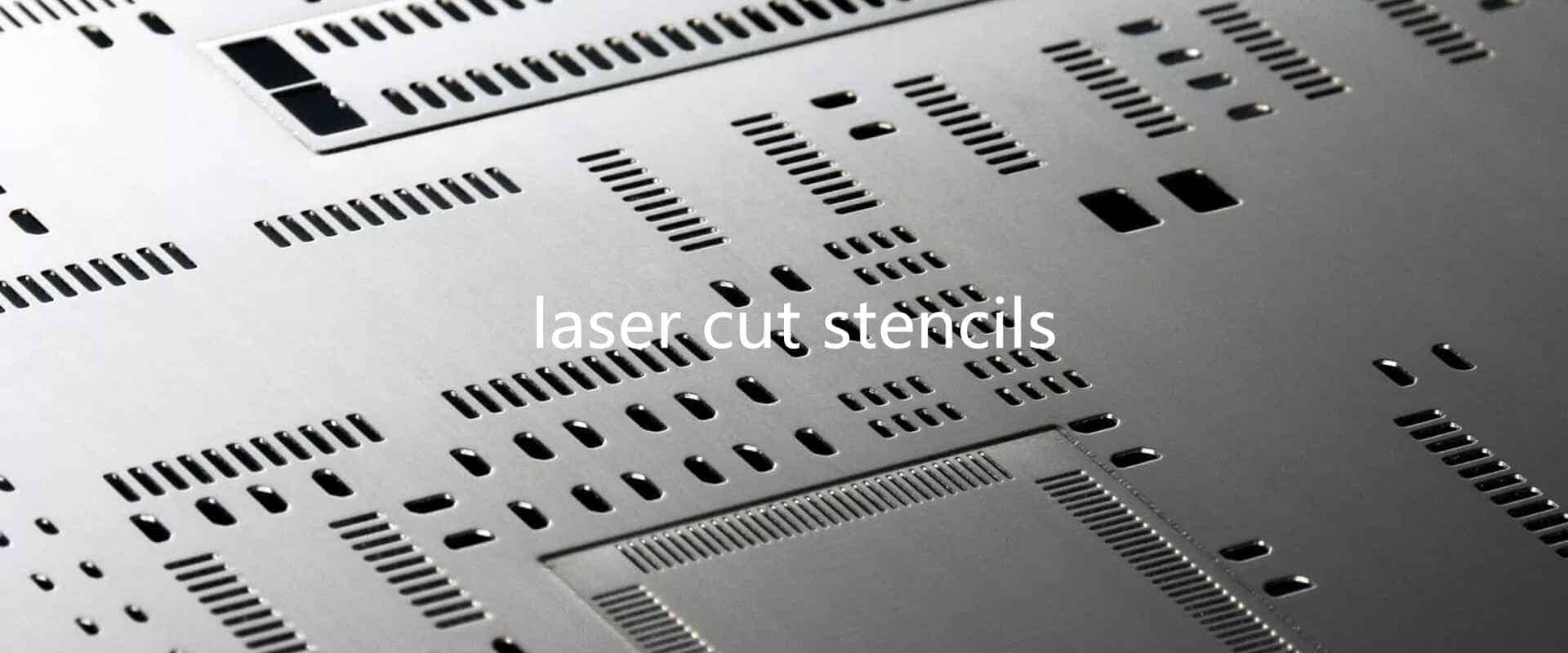
- Laser cut stencils – A CO2 laser cuts the stencil apertures into stainless steel or brass foil. Offers good precision at lower costs.
- Electroformed stencils – Metal is selectively plated onto a substrate to create apertures. Provides highest precision but at higher costs.
- Electropolished stencils – Electrochemical polishing smoothens cut edges for clean aperture walls and easier paste release.
- Step stencils – Foil thickness steps down around smaller apertures to optimize paste deposits.
- Nano-coated stencils – Thin chemical coatings reduce surface energies for effortless paste release without sticking and bridging.
- Dual layer stencils – Two metal foil layers provide both large and small apertures to optimize printing.
- Hybrid laser cut stencils – Combines laser cutting and electropolishing for a cost-effective but high performance stencil.
- Mini stencils & step stencils – Designed for printing paste onto individual PCBs separated in panels, rather than full panels.
- Foil stencils – Low cost stencils with basic rectangular laser cut apertures for low volume and prototype PCB assembly.
Selecting the right stencil type depends on factors like production volume, PCB complexity, aperture sizes, fine pitch density, planarity, and budget.
What materials are used to manufacture PCB stencils?
The most common PCB stencil materials are:
- Stainless Steel – Most widely used for its durability, dimensional stability, and ease of cleaning. 304 and 316 grade steel with electropolish finish.
- Brass – A soft metal alloy that offers good paste release. Commonly used for laser cut stencils.
- Nickel Plated metals – Nickel coating on stainless steel or brass aids paste release. Provides durability over brass alone.
- Polyimide – Advanced polymer stencils with laser cut apertures. Used for PCB prototyping and ultra fine pitch ICs.
- Aluminum – Lightweight but tends to warp and scratch easily so limited use.
- Metal composite – Multi-layer metal foils combine properties like durability, stability and paste release.
Stainless steel is ideal for most stencil applications. Brass, nickel plate, and composites suit more challenging paste release needs. Polymer stencils work for low volume prototyping. The material impacts stencil lifetime, print quality, and cost.
What are the key parameters for designing a PCB stencil?
Some of the key design considerations when creating a PCB stencil are:
| Parameter | Description |
|---|---|
| Aperture dimensions | Apertures match PCB pads for accurate paste transfer. Aperture widths are adjusted to optimize paste deposits. |
| Land to stencil ratios | The ratio between stencil aperture size to pad size ranges from 1:1 to 0.66:1. Wider areas may use larger apertures. |
| Stencil thickness | Typical 2 to 8 mil thickness. Thicker stencils deposit more paste but can cause bridging. Thinner stencils reduce bridging but deposit less paste. A step stencil may be used. |
| Tolerance and roughness | Tighter tolerances of +/- 5 microns on etched stencils improve alignment and print definition. Smooth stencil walls from electropolish improve paste release. |
| Aspect ratio | The ratio of stencil thickness to stencil aperture size. Higher aspect ratios above 0.66 can cause paste release issues. |
| Snap off reduction | Small tabs connect islands in stencil apertures to prevent them breaking off when handling and cleaning thin stencils. |
| Other features | Additional nose ports, glue dots, and edge bead compensation improve paste release and reduce bridging and solder balls. |
Stencil design requires balancing many parameters to achieve good solder paste print definition, appropriate paste volumes, and high yields.
What is the typical PCB stencil fabrication and manufacturing process?
PCB stencils are fabricated using precision processes to create metal foil sheets with accurately defined apertures:
- Start with metal foil raw material of desired thickness and dimensions. Stainless steel foils are commonly used although brass, nickel-plated brass and composite foils are alternatives.
- Clean and prepare the foil surface for processing. This improves surface finish and adhesion of any coatings to be applied.
- Create stencil design file defining all apertures using CAD software.
- Use photolithographic mask and chemical etch processes to corrode away unwanted metal to form apertures. Repeat coating, imaging and etching stages may be used.
- For higher precision, use laser or micro-machining methods to ablate away metal foil and cut out stencil openings.
- Use electropolishing to smooth cut aperture walls and even out thickness variations for consistent paste release.
- Apply proprietary nanocoatings as needed to further enhance paste release characteristics.
- Add laser cut tabs, fiducials and other stencil features for ease of handling, alignment and cleaning.
- Mount the finished stencil foil onto a frame for insertion into stencil printers.
Precision fabrication maximizes stencil accuracy and capabilities for depositing solder paste onto PCBs during SMT assembly.
What are the key steps in using a PCB stencil?
Using a stencil to apply solder paste to a PCB involves several important steps:
- Stencil cleaning – Clean any residual paste from previous print runs using wipe, spray or ultrasonic methods. This prevents particle accumulation clogging apertures.
- Stencil mounting – Attach the stencil to the stencil printer using the appropriate frame and securing mechanisms.
- PCB loading – Load the PCB into the printer and align it precisely to the stencil. Use split vision cameras for accuracy.
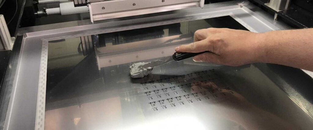
- Solder paste application – Roll paste across stencil surface using a squeegee to fill apertures. Apply even pressure for uniform fill.
- Print stroke – Lower stencil onto PCB then lift off again, leaving paste deposits. Slow, steady stroke speeds aid paste release.
- Inspection – Inspect paste deposits and print quality. Optimize settings to correct any issues.
- Releasing PCB – Unload the PCB from the printer for next steps of component placement and reflow.
Proper setup, calibration, operating procedures and inspection are key to achieving high solder paste printing yields with the stencil.
What are some common defects in stencil printing?
Some typical defects that can occur with PCB stencil printing include:
- Bridging – Solder paste bridges between adjacent pads. Caused by too much paste, aperture misalignment or damaged stencil walls.
- Insufficient paste – Too little paste applied due to low stencil thickness, blocked apertures or poor release performance.
- Solder balls – Small blobs of paste stuck to PCB after printing. Results from sticky paste or high separation speeds.
- Smearing – Blurred uneven paste deposits due to misaligned stencil, poor snap-off, or high print speeds.
- Missing paste – No paste deposited on some pads due to blocked stencil apertures or damaged stencil.
- Poor co-planarity – Uneven paste height due to un-level stencil, poor board support or non-uniform paste volume.
- Registration errors – Shifted, rotated or skewed paste prints arising from inaccurate stencil alignment.
With careful process controls and stencil maintenance, defects can be minimized to achieve high PCB assembly yields.
How often does a PCB stencil need cleaning?
PCB stencils require regular cleaning to prevent solder paste and particulates from accumulating and degrading print quality:
- Stencils should be cleaned after every 50-100 print strokes. More frequent for very fine pitch prints.
- Stencils may be wiped after every 5-10 print strokes to remove large debris and ensure good quality.
- Cleaning is needed after extended production halts of 8 hours or more. Dried paste can clog apertures.
- End-of-day cleaning is recommended to prevent paste hardening overnight which can block apertures.
- Weekly cleaning using ultrasonics or aggressive wipes helps remove hardened paste residue.
- New or reworked stencils need cleaning before first use to remove any contaminants.
More frequent cleaning improves paste release, reduces particle buildup, and mitigates print defects. However, excessive cleaning can damage stencils. Finding the right cleaning balance optimizes stencil lifetime and performance.
What are the different methods for cleaning PCB stencils?
Common cleaning methods for PCB stencils include:
- Dry wipes – Manual wipes or automated roller cleaners with cleaning paper or soft cloths to remove paste. Low cost but less effective for hardened paste.
- Wet wipes – Wipes moistened with cleaners such as isopropyl alcohol for added cleaning power to remove stuck-on contaminants.
- Spray cleaners – Solvent sprays or saponifiers applied to the stencil to break down paste residues. Wipes follow to remove.
- Ultrasonic cleaners – Stencils submerged in solution and ultrasonically agitated to thoroughly clean. Most effective method but slower.
- Stencil wipe stations – Dedicated machines combining wiping, spraying and vacuuming for automated cleaning between prints. Fast process integrated into printing.
- Laser cleaning – Modified lasers pulse controlled energy onto stencils pyrolytically decompose and remove paste residues. Very effective yet expensive option.
Selecting suitable cleaning methods and media prevents damage while thoroughly removing paste and particulates for high quality solder paste deposition.
What factors affect the lifetime and durability of a PCB stencil?
A PCB stencil’s lifespan depends on several factors:
- Cleaning methods – Harsh scrubbing and ultrasonics wear the stencil prematurely if not done properly.
- Handling and storage – Dents, bending or scratches from mishandling reduce stencil life. Proper storage in clean, protected environment extends lifespan.
- Aperture dimensions – Very small apertures below 100 microns wide see faster wear around fragile walls.
- Foil thickness – Durability reduces below 3 mil thickness while thicker 8+ mil foils withstand damage better.
- Solder paste – Highly abrasive paste formulas cause more wear during printing and cleaning.
- Material properties – Softer metals like brass are more prone to damage than hardened stainless steel. Nickel plating aids durability.
- Coatings – Anti-static and chemically inert nano-coatings protect materials from chemical or physical damage.
- Usage frequency – Stencils in high volume production see faster wear versus prototyping uses.
With careful handling and optimal materials and coatings, stencils can last hundreds of thousands of print cycles before needing replacement.
What are some best practices for PCB stencil maintenance?
Some recommended best practices for maintaining PCB stencils include:
- Store stencils properly in clean, dry, anti-static packaging when not in use. Avoid humidity, debris, and physical damage.
- Clean stencils regularly using optimal methods to remove paste but not abrade the foil. Utilize wipe stations for fast automated cleaning.
- Inspect stencils under magnification routinely for damage, especially around thin, fragile aperture walls prone to issues.
- Replace worn or damaged stencils where print quality is compromised. Repairs may be possible in some cases.
- Monitor and optimize solder paste roll, separation speed, and other print parameters to reduce defects and extend stencil lifetime.
- Apply fresh anti-static, chemical resistant nano-coatings after cleaning to restore non-stick, non-abrasive properties.
- Ensure proper frame mounting, PCB support, and release film usage to minimize damage from board separation.
- Perform periodic understencil cleaning and increasing wipe pressure/frequency to clear any developing clogs.
Proper maintenance maximizes a stencil’s usable life, reduces defects, and sustains print quality and performance.
What are some recent trends and developments in PCB stencil technology?
Some latest trends shaping PCB stencil technology include:
- Laser cut stencils with more precision, faster speeds, and reduced costs making them viable for higher mix production.
- Nano coatings such as fluoropolymers that significantly improve paste release while protecting stencils.
- Stencil gasketing integrated into the stencil to seal and mount directly to the PCB for consistent clearances.
- Automated optical inspection of stencil aperture integrity and paste deposits to rapidly flag any print issues.


Leave a Reply