Introduction
PCB stands for printed circuit board. PCBs are the fundamental building blocks of all modern electronics hardware. Understanding what PCBs are and how they work is essential knowledge for anyone involved in electrical engineering, circuit design, and embedded system development.
This comprehensive guide will explain everything you need to know about PCBs including:
- PCB definition and history
- PCB design and layout
- PCB materials and construction
- PCB fabrication process
- PCB assembly and prototyping
- PCB design software
- Advantages of using PCBs
- Applications and usage of PCBs
Let’s dive in and demystify this critical component that powers electronics as we know it!
PCB Definition
A printed circuit board or PCB is a non-conductive substrate used to mechanically support and electrically connect electronic components using conductive copper traces and pads. The circuits connecting components are printed onto the PCB through a variety of printing and etching techniques.
PCBs provide a stable base for mounting both surface mount and through-hole components. Conductive layers in the board then allow current to flow between attached components to form functioning electronic circuits. PCBs are ubiquitous in all electronic devices and systems.
Brief History of PCBs
The earliest predecessors to PCBs were used in the 1850s for mounting components and connecting wiring in telegraph systems. Printed single-sided circuit boards started appearing in the early 20th century. In 1925 Charles Ducas is credited with printing an early circuit pattern using an etching process.
The PCB field greatly expanded with the patenting of double-sided plates in 1943 by John Sargrove, allowing increased circuit complexity. Increasing military needs during World War II drove rapid improvements in PCB technology and fabrication throughout the 1950s and 60s. Consumer electronics boom further spurred PCB adoption and innovation in the 70s and 80s.
Modern surface-mount technology, multilayer boards, and PCB miniaturization have enabled the continuously advancing capabilities and compact form factors of modern electronics. PCBs have been instrumental in enabling this progress.
PCB Design and Layout
The specific layout of traces, pads, vias, holes, layers, and other features on a PCB is known as the PCB design. It serves as the blueprint for fabrication. Good PCB design adheres to many parameters:
- Electrical connectivity requirements
- Component placement for usability and assembly
- Efficient routing to minimize layers and vias
- Controlled impedance for high speed signals
- EMI/EMC protections against interference
- Thermal management strategies for cooling
- Minimizing board space usage
PCB layout involves carefully translating the electronic circuit schematics into board geometry within manufacturing and performance constraints. PCB layout tools assist designers in this complex task.
PCB Materials and Construction
A PCB consists of multiple layers of different materials laminated together:
- Substrate – Provides mechanical base for PCB. Usually fiberglass-reinforced epoxy laminate FR-4. Can also be rigid-flex, PTFE, etc.
- Conductors – Copper foil provides conductive pathways on one or both sides of substrate.
- Dielectrics – Prepreg bonding material used to separate and glue conductor layers.
- Coatings – Such as solder mask, silkscreen, finishes that protect and label the PCB.
Vias and plated through holes provide conductivity between layers in multilayer PCBs. Additional components like integrated circuits, resistors, capacitors etc. are mounted onto the PCB surface to form a complete circuit.
PCB Fabrication Process
PCBs are manufactured by specialist board houses using processes like:
- Lamination – Gluing substrate and foil layers together under heat and pressure
- Drilling – Creating via holes through the board
- Plating – Electroplating conductive walls in drilled vias
- Imaging – Photolithography to transfer layout patterns onto layers
- Etching – Chemically etching away unwanted copper
- Solder mask – Applying epoxy coatings as solder and scratch protection
- Silkscreen – Printing reference labels on the board
- Testing – Electrical testing and inspection
Mass production PCBs are fabricated using these complex processes in panelized format for efficiency. Improved fabrication technology enables ever-finer features and multilayer boards.
PCB Assembly and Prototyping
After fabrication, PCB assembly involves:
- Solder paste application
- Pick-and-place of surface mount components by robotics
- Reflow soldering in ovens
- Manual insertion of connectors and through-hole components
- Conformal coating for protection
- Programming firmware
- Functional testing
For prototypes, PCB assembly uses more manual workflow including hand soldering and through-hole parts. Small-batch PCB assembly services bridge the gap between prototypes and mass production.

PCB Design Software
To design PCB layouts efficiently, electrical engineers use EDA software tools like:
- KiCad – Open source, comprehensive for schematic capture and PCB layout
- Eagle – Very popular, now owned by Autodesk
- Altium – Advanced tools for high complexity, high cost
- OrCAD – Part of Cadence tool suite, more legacy userbase
- Pads – Feature rich, owned by Mentor graphics
These tools provide design rule checking, autorouting, 3D visualization, and integration for manufacturing.
Advantages of Using PCBs
Here are some of the key benefits that make PCBs a ubiquitous foundation of electronics:
- Compact – PCBs allow dense mounting of components and routing of traces
- Reliable – Robust base for securely mounting components
- Scalable – Additional layers accommodate more complex circuits
- Standardized – Mature industry with defined fabrication processes
- Automatable – Highly repeatable manufacturing and assembly
- Repairable – Relative ease of troubleshooting and fixing issues
- Upgradable – Layouts and components can evolve across generations
Applications and Usage of PCBs
Virtually every electronic device relies on PCBs:
- Consumer electronics – Phones, laptops, gadgets
- Appliances – Washers, microwaves, fridges
- Automobiles – Engine controllers, infotainment
- Aerospace – Avionics, instrument panels
- Industrial – PLCs, process control, test equipment
- Medical – Patient monitors, imaging, diagnostics
- Military – Radios, displays, GPS, sensors
- Smart Infrastructure – Traffic signals, security, IoT
The applications are incredibly diverse because PCBs can pack intelligence and connectivity into nearly any object. PCBs will continue growing more advanced and pervasive going forward.
FQA
What are the different types of PCBs?
Some common categories of PCBs include:
- Single-sided – Conductors only on one side
- Double-sided – Conductors on both sides
- Multilayer – Multiple conductor layers laminated together
- Rigid PCBs – Standard rigid fiberglass substrate
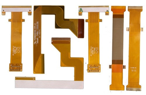
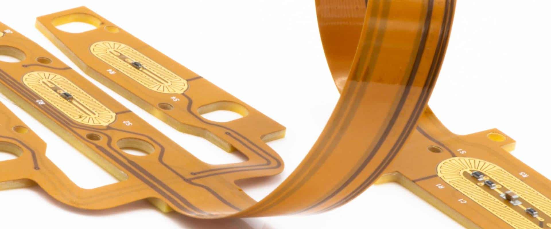
- Flex PCBs – Flexible polyimide substrate
- Rigid-flex – Combines both rigid and flex sections
- HDI – High density interconnect with very fine features
How are PCB layout files generated?
PCB layout files are designed using EDA (electronic design automation) software tools. The designer first creates schematics to define the electronic circuits. PCB layout is then completed, often aided by autorouting. The EDA tool outputs layout files like Gerbers for fabrication.
What are some differences between through-hole and surface mount PCB technology?
Through-hole parts have leads that mount through holes in the PCB. Surface mount or SMT parts directly mount to pads on the top surface. SMT allows higher component density but requires solder paste and reflowing. Through-hole is easier to hand assemble but takes more space.
How accurate and small can PCB traces and spaces be fabricated?
High end PCB technology supports trace/space dimensions below 5 mils (0.127mm) and tolerances within 2 mils. Main limitations are number of layers, board thickness, and minimum copper weight. Better fabrication improves accuracy of fine features.
How should I clean flux residue off PCBs after soldering?
You can use cotton swabs and isopropyl alcohol >90% to gently clean PCBs after soldering. Take care not to be overaggressive and damage any components or lifted pads. Avoid touching the board until completely dry. For no-clean flux, cleaning is often not necessary.
Summary
I hope this guide has clarified what exactly a PCB is, how they are designed and manufactured, why they are so ubiquitous in electronics, and the many applications they enable. PCBs form the backbone of modern electrical engineering and play a critical role in nearly all electronic devices we use daily. Understanding PCB technology is an important foundation for working in embedded systems, IoT, consumer electronics, aerospace, medical, and related high tech fields.


Leave a Reply