Ceramic printed circuit boards (PCBs) provide unique capabilities that make them ideal for many demanding applications. Ceramic PCBs boast exceptional thermal performance, mechanical strength, chemical resistance, and electrical insulation properties unmatched by traditional fiberglass PCBs. These characteristics enable ceramic PCBs to excel in high reliability systems across automotive, aerospace, industrial, medical, and other sectors.
Overview of Ceramic PCBs
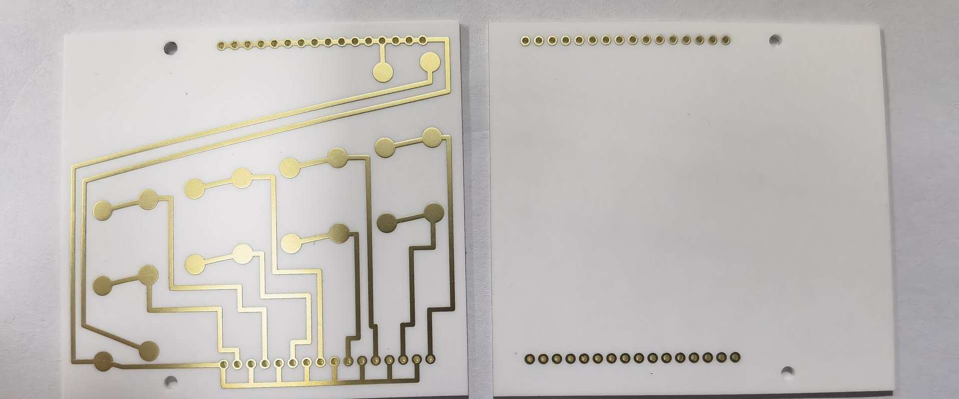
Ceramic PCBs use ceramic materials as the insulating substrate instead of the more common fiberglass or other laminate materials. Popular ceramic options include aluminum oxide, aluminum nitride, and beryllium oxide. These create extremely hard, heat-resistant boards able to withstand very high temperatures, voltages, frequencies and other stresses.
The ceramic itself forms the foundation layer, upon which conductive traces and pads are added, usually by a thermal spray deposition process. Components are soldered onto the PCB as normal. The result is a rugged board that resists cracking and performs reliably in demanding conditions.
Unique Properties of Ceramic PCBs
Ceramic PCBs offer several capabilities that surpass other PCB technologies:
Thermal conductivity – Ceramic has far higher thermal conductivity than fiberglass, allowing ceramic PCBs to dissipate heat extremely effectively. This makes them suitable for high power applications.
Temperature resistance – Withstanding temperatures exceeding 1000°C, ceramic PCBs work reliably at very high temperatures that would damage other boards.
Structural rigidity – Hardness and stiffness of ceramic gives excellent mechanical strength and resistance to vibration or shock.
Chemical inertness – Ceramic is impervious to most corrosive chemicals and solvents unlike traditional laminates.
Electrical insulation – The ceramic substrate provides very effective insulation even at high voltages, with low loss.
Miniaturization – Thin ceramic layers allow creation of boards with very fine lines and spaces for dense, microscale circuits.
Hermetic sealing – Ceramic’s non-porous nature enables hermetic PCB sealing for sensitive devices like MEMS.
These exceptional performance attributes make ceramic PCB technology ideal for many niche applications.
Typical Applications of Ceramic PCBs
Here are some common applications benefiting from ceramic PCB capabilities:
High Temperature Electronics
Ceramic PCBs enable electronics to operate at very high temperatures exceeding 660°F (350°C) such as downhole drilling equipment, Venus surface probes, turbine engine controls, and nuclear systems monitoring electronics. Fiberglass PCBs would char and burn at such temperatures.
High Frequency and High Speed Circuits
The excellent electrical insulation and low losses of ceramic substrates allow ceramic PCBs to work with frequencies exceeding 10 GHz. This makes them well-suited for microwave radio equipment, radar systems, satellite communication, and other high frequency needs.
Power Electronics
The thermal conductivity of ceramic PCBs is hundreds of times higher than fiberglass, making heat dissipation very effective. This allows high power density circuit designs ideal for power supplies, motor drives, HVDC converters and similar applications.
High Voltage Electronics
Ceramic’s high electrical resistance permits ceramic PCBs to withstand very high voltages above 25kV. This enables their use in X-ray generators, pulsed power systems, or experimental physics applications using intense electric fields.
Low Noise Sensitive Circuits
The hard ceramic substrate prevents microphonic noise issues caused by vibration interfering with sensitive analog sensors or precision reference circuits. The excellent insulation also offers very low electromagnetic interference.
MEMS Sensors and Actuators
Ceramic PCBs can create hermetically sealed cavities for microelectromechanical systems (MEMS) like accelerometers, gyroscopes, or micromirror devices. This provides reliable encapsulation of the microscale mechanics.
Corrosive Environments
The imperviousness of ceramic to corrosive chemicals like acids, solvents or petroleum means ceramic PCBs survive environments that would rapidly degrade traditional PCB laminates.
Medical Implants and Prosthetics
The biocompatibility and hermetic sealing ability of ceramic makes it suitable for PCBs used in active medical implants like cochlear implants or stimulators needing long-term performance and biological isolation.
Aerospace and Defense
Ruggedness, miniaturization capability, and tolerance of intense vibration, shock, temperature, and radiation makes ceramic PCBs ideal for space systems, munitions, and other extreme military electronics applications.
For electronics pushing the limits, ceramic PCB technology enables reliable, robust solutions where other PCB materials would fail. Their unique strengths open up capabilities beyond standard boards.
Ceramic Materials Used in PCBs
Several specific ceramic materials are commonly used to fabricate ceramic PCB substrates:
Aluminum Oxide – Al2O3
- Also called alumina
- Most popular and cost effective choice
- High strength and stiffness
- Resists temperature, chemicals, and wear
- Moderate thermal conductivity
Aluminum Nitride – AlN
- High thermal conductivity for heat dissipation
- Low thermal expansion coefficient
- Withstands 600°C temperatures
- High frequency capability above 10 GHz
- More expensive than alumina
Beryllium Oxide – BeO
- Exceptional thermal conductivity
- Very low dielectric loss
- Handles high power density
- Toxicity requires careful handling
- Controlled material due to radiation usage
Silicon Nitride – Si3N4
- Combines high strength with thermal capability
- Fracture and shock resistance
- Operates up to 1000°C
- Relatively new option for PCBs
- Being adopted for electric vehicle and 5G uses
Zirconia – ZrO2
- Extremely hard and resistant to wear
- Fracture toughness and durability
- Useful for demanding mechanical applications
- Lower thermal conductivity than other ceramics
Material choice depends on tradeoffs between thermal, mechanical, electrical, and cost priorities. Most boards use alumina or aluminum nitride. Beryllium oxide is avoided if possible. Different material formulations are also used to customize properties.
Ceramic PCB Construction and Fabrication
Ceramic PCBs have a specialized fabrication process tailored to the properties of the ceramic materials. Here is an overview of construction:
Ceramic Substrate – The base layer is made from fired ceramic tape or pressed ceramic powder. This forms a flat, smooth substrate for subsequent layers.
Metalized Traces – Conductive traces are applied on the ceramic substrate using processes like direct copper bonding, thin film deposition, or metal spraying.
Vias – Holes are laser drilled and filled with conductive material to form vertical interconnects between layers.
Lamination – Multiple thin cofired ceramic layers, trace layers, and via interconnects are stacked up and laminated under pressure to form multilayer boards.
Component Assembly – Leaded or leadless components are attached to the PCB surface usually via soldering.
Sealing – For boards needing hermetic sealing, the cavities are sealed with lids using welding, eutectic bonding, or brazing.
The specialized materials and processes result in a rugged PCB assembly able to withstand much higher temperature, power, and other stresses than conventional boards.
Design Considerations for Ceramic PCBs
Designing for ceramic PCB technology requires attention to the unique capabilities and constraints:
- Account for reduced flexural strength and fracture toughness compared to organic boards
- Thermal expansion mismatches between components, solders, and ceramic require analysis
- Allow wider spacing and isolation gaps due to material hardness
- Vias can crack from drilling stress so should have larger diameters
- Higher processing temperatures impact material choices for conductors, solders, and components
- Hermetic sealing may require vent holes for gas escapes during sealing
- Thinner and more numerous layers are possible compared to traditional PCBs
- Warpage can occur in unfired ceramic during processing which affects tolerances
- Shrinkage of around 15% occurs when firing ceramic layers
- Higher costs involved due to specialized materials and fabrication processes
Designing with the properties, precision, and constraints of the ceramic PCB process ensures successful boards.
Ceramic PCB Cost Considerations
Ceramic PCB technology has higher costs than standard PCB approaches:
- Materials – Raw ceramic substrate materials cost more than typical laminates
- Processing – Firing, vacuum deposition, and other fabrication steps are expensive
- Volume – Much lower economies of scale compared to mass-produced PCBs
- Tooling – Fabrication equipment like lasers and metalizers required
- Yield – Tighter tolerances and conventional PCBs make yields lower
- Testing – 100% electrical testing often needed due to cost of failures
- Changeovers – Setup for different layer counts, materials adds expense
However, for many applications the performance benefits outweigh the higher price. And as manufacturing scales up, costs can decrease significantly.
Ceramic PCB Challenges and Limitations
Some limitations to consider with ceramic PCB technology:
- Cost – Higher cost restricts applications due to specialized materials and processes
- Lead times – Fabrication requires considerable processing time
- Fragility – Prone to cracking or fracturing compared to organic boards
- Size limits – Standard sizes smaller than large fiberglass boards
- Low layer count – Typically 10 layers or less versus 20+ on advanced PCBs
- Via drilling – Making clean, high density small vias can be difficult
- Fine features – Line width and spacing not as fine as leading edge PCBs
- Mixed assemblies – Combining with standard PCBs requires analysis for matching
Ceramic PCBs thus tend to be used only where their specific capabilities are required. Conventional PCBs handle cost-sensitive, high volume commodity needs.
Future Developments for Ceramic PCBs
Several technology trends will expand ceramic PCB adoption:
- Manufacturing improvements – Higher volume production and yield increases bringing costs down
- 5G infrastructure – High frequency mmWave hardware needs low-loss ceramic PCBs
- Electric vehicles – More complex powertrain electronics require thermal performance
- Aeronautics – Advanced aircraft and space systems moving to ceramic PCBs
- Medtech – Implantable devices benefitting from biocompatible ceramic PCBs
- Embedded computing – Dense SBCs with high core counts demand ceramic cooling
While ceramic PCB technology has been niche, its unique capabilities are becoming more crucial for leading-edge applications. Continued improvements and new uses will drive expanded adoption.
FQA about Ceramic PCBs
Here are answers to some frequently asked questions about ceramic PCB technology:
Q: What are the main advantages of using ceramic instead of FR4 in PCBs?
A: The advantages include:
- Extremely high thermal conductivity for heat dissipation
- Ability to withstand very high temperatures over 1000°C
- Hermetic sealing capability for sensitive devices
- Improved high frequency characteristics at microwave frequencies
- Withstands intense vibration, shock, and acceleration forces
- Resists virtually all solvents, acids, and chemicals
Q: What types of electronics applications benefit the most from ceramic PCBs?
A: Applications benefiting include:
- Downhole oil drilling tools and high temperature industrial uses
- Medical implants needing biocompatibility and hermetic sealing
- Aerospace and automotive electronics seeing intense vibration
- High power density electronics like power supplies and converters
- High frequency microwave and mmWave wireless hardware
- Any system needing high reliability in extreme environments
Q: What are the downsides or tradeoffs when using ceramic instead of FR4 PCBs?
A: Drawbacks include:
- Much higher cost due to specialized materials and processes
- Larger minimum feature sizes and lower layer counts
- Increased fragility and lower fracture toughness
- Longer fabrication lead times for processing
- Higher weight compared to lightweight laminates
- Difficulty drilling small vias and holes through hard ceramic
Q: Are there particular design considerations needed when designing a ceramic PCB?
A: Considerations include:
- Having larger spacing between features due to less precise fabrication
- Minimizing use of small vias by having fewer layers
- Managing thermal expansion mismatches in components and joints
- Adding strengthening features to mitigate fragility risk
- Using wider traces for high current handling due to heat
- Allowing sufficient clearance for high voltage isolation
Q: What new applications are emerging that can benefit from ceramic PCB capabilities?
A: New applications:
- Electric vehicle power electronics as complexity increases
- 5G wireless infrastructure at mmWave frequencies
- Aerospace electronics like engine controls and avionics
- High density processing modules with multiple processors
- Medical implants as they become more sophisticated
- Robust industrial automation systems in harsh factories
The extreme performance abilities of ceramic PCBs make them well suited for leading-edge systems pushing boundaries.


Leave a Reply