Introduction
Designing printed circuit boards (PCBs) involves a number of key steps and stages to transform circuit requirements into a physical board layout ready for fabrication and assembly. This comprehensive guide will walk through the complete PCB design process from concept to completion.
By the end, you’ll have a clear understanding of the sequential tasks and workflows required to design boards using electronic design automation (EDA) software. We’ll cover everything from initial schematic capture through final output generation in detail.
Understanding these fundamental PCB design steps provides the foundation for creating successful boards in any application across consumer, industrial, medical, aerospace/defense, automotive, and other industries.
Overview of the PCB Design Process
At a high level, the core stages in PCB design are:
Schematic Capture
- Create circuit schematic detailing components and connectivity
PCB Layout
- Transform schematic into physical board layout
Design Verification
- Validate design integrity through testing and analysis
Manufacturing Outputs
- Generate Gerber, drill, BOM, fabrication/assembly files
This simplified workflow provides the skeleton for the complete PCB design process. Now let’s explore each stage more deeply.
Schematic Capture
Schematic capture involves developing the electronic circuit schematic that defines the board’s functionality. This includes:
1. Create Component Symbols
- Generate symbols for all ICs, transistors, diodes, etc.
2. Place Symbols
- Arrange components on the sheet
3. Connect Symbols
- Draw wires connecting component terminals
4. Apply Net Names
- Label each network/connection
5. Add Power Connections
- Show power inputs, ground, decoupling
6. Create Hierarchical Sheets
- Link sheets for complex designs
7. Attach Component Properties
- Fill in part numbers, values, footprints
8. Add Notes and Guidelines
- Additional markup and documentation
The schematic capture stage fully describes the circuit’s operation and components. This drives the subsequent PCB layout.
PCB Layout
With the schematic completed, the layout stage transforms the logical connnectivity into a physical PCB design.
1. Place Components
- Position parts based on schematic
2. Route Traces
- Connect pads with copper traces
3. Define Layers
- Assign signal layers, plane layers
4. Add Dimensions
- Board outline and component locations
5. Place Vias/Pads
- Connect between layers
6. Assign Net Classes
- For trace width rules
7. Route Power
- Connect power across layers
8. Route Signals
- Follow topology in schematic
9. Route critical traces
- High speed signals, matched lengths
10. Route Remaining Traces
- Complete trace connectivity
11. Complete Layout
- Finalize all board geometry
Meticulous PCB layout translates the circuit schematic into a routable design that can be manufactured.
Design Verification
Before manufacturing, the PCB layout undergoes verification and testing:
1. Design Rule Check
- Validate trace widths, spacings, etc
2. Electrical Rules Check
- Confirm net connections match schematic
3. Signal Integrity Analysis
- Assess high speed signal quality
4. Power Integrity Analysis
- Review power distribution
5. Thermal Analysis
- Ensure components within temperature limits
6. Generate Netlist
- Export netlist for comparison
7. Perform EMI Analysis
- Check electromagnetic interference
8. Validate Manufacturability
- Confirm board is fabricable as designed
9. Review Layout
- Comprehensive design review
This rigorous verification process avoids costly mistakes reaching board fabrication.
Manufacturing Outputs
With design complete, manufacturing output files are generated:
1. Gerber Files
- Layer-by-layer board fabrication data
2. Drill Files
- Locations for holes and vias
3. Component Placement Files
- Pick-and-place data for assembly
4. BOM File
- Parts list, reference designators
5. Assembly Drawings
- Mechanical assembly diagrams
6. Schematics/Block Diagrams
- Printed schematics for documentation
7. Readme File
- Design notes, instructions, settings
These outputs hand off everything needed for smooth board fabrication, assembly, and testing.
Advanced and Optional Steps
For more complex boards, additional possible steps include:
- Simulation with analog/digital models
- Creating complex pad shapes
- Adding internal cutouts and mechanical features
- Designing impedance controlled traces
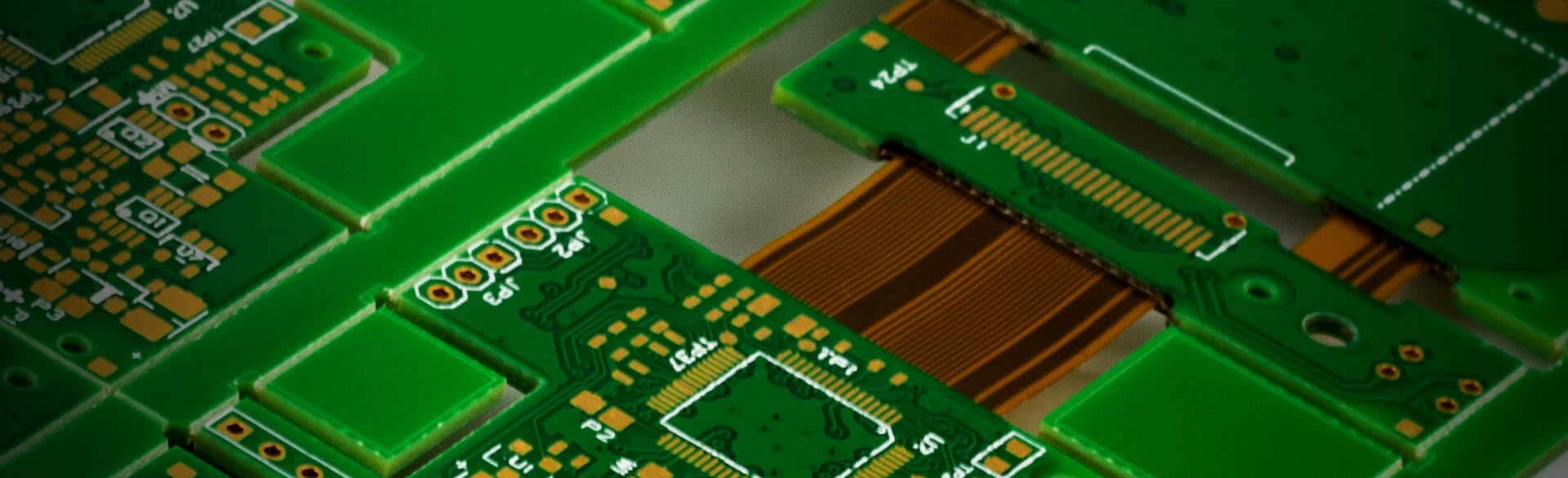
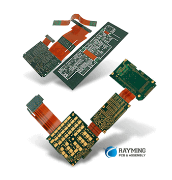
- Importing rigid-flex CAD data
- Embedding thermal reliefs for traces
- Adding testpoints, fiducials, and tooling holes
- Creating custom footprints for unique components
- Designing multilayer stacks with blind/buried vias
- Capturing board variations through configurations
This covers some less common tasks that may be involved for high complexity boards.
Key PCB Design Stages Summary
To recap, the core worklow of PCB design consists of:
- Schematic Capture – Develop circuit schematic
- PCB Layout – Transform into physical layout
- Verification – Validate pre-manufacturing
- Outputs – Generate fabrication/assembly files
Additional steps can augment this core flow depending on design complexity, analysis needs, and other factors.
Now let’s look at some different ways to organize this PCB design process.
Linear vs Iterative Approaches
There are two general approaches to managing the PCB design workflow:
Linear Methodology
Involves completing each stage sequentially before moving to the next. For example:
- Finish schematic capture
- Complete PCB layout
- Perform design verification
- Generate manufacturing outputs
This linear progression minimizes iterations by finalizing each step before proceeding.
Iterative Methodology
Uses a cyclic approach allowing revisiting previous stages as needed. For example:
- Draft schematic
- Start PCB layout
- Revise schematic
- Update PCB layout
- Verify design
- Repeat changes as needed
The iterative approach expects revisions between steps rather than a purely linear flow.
In practice, PCB design usually involves some combination of these methodologies, with upfront planning smoothing iterations later in the cycle.
Top Down vs Bottom Up Approaches
In addition to linear vs iterative, PCB design can follow “top down” or “bottom up” workflows:
Top Down
Starts by fully defining requirements and architecture before implementation.
- Specify design goals, constraints, interfaces
- Map system architecture and decomposition
- Allocate requirements to sub-systems
- Flow down key parameters
- Define schemas, budgets
Bottom Up
Begins practical development first, then derives architecture.
- Create draft schematics of key circuits
- Develop prototype modules and blocks
- Evaluate technical capability
- Determine detailed requirements based on prototypes
- Synthesize higher level architecture
Most designs use some blend of top down guidelines and bottom up prototyping. The best balance depends on the specific project.
Role of Design Reviews
Reviews and inspections should occur at key milestones through the PCB design process. Typical design reviews include:
- Concept Review – Evaluate proposed approach/architecture
- Schematic Review – Verify circuit design before layout
- Layout Review – Review board artwork before tapeout
- Verification Review – Inspect results of analysis and testing
- Pre-Tapeout Review – Final check before manufacturing release
Reviews provide formal oversight checkpoints and help avoid oversights. Cross-functional team reviews are ideal to leverage diverse expertise.
Optimizing the Design Process
To maximize efficiency, important factors include:
- Requirements – Well-defined ahead of implementation
- Planning – Clear schedule and task sequence
- Communication – Align team on status and issues
- Collaboration – Effective handoffs between steps
- Revision Control – Disciplined change management
- Automation – Scripting, macros to accelerate workflows
- IP Reuse – Leverage existing validated blocks
- Tool Expertise – Learn software capabilities in depth
- Project Management – Systematic tracking and oversight
Focusing on these aspects helps smooth the inherently complex PCB design process.
Conclusion
This guide reviewed the typical stages and steps involved in completing PCB designs:
- Schematic capture of the electronic circuit
- Physical layout transforming the schematic
- Verification through testing and analysis
- Manufacturing output generation
- Supplemental workflow approaches and considerations
By understanding this overall design process and the tasks encompassed within each phase, PCB designers can plan and execute board designs efficiently.
The exact steps required for a given design depend on many factors including complexity, team experience, timelines, review requirements, and availability of qualified EDA software tools. But following the fundamental workflow provides a roadmap to transforming circuit requirements into manufacturable board designs.
Frequently Asked Questions
What are the 5 main steps in the PCB design process?
The 5 high-level main steps are:
- Creating the schematic
- Laying out the board layout
- Verifying the design
- Generating manufacturing outputs
- Tapeout release for fabrication
What is the first step in designing a PCB?
The first step is schematic capture. This involves drafting the electronic circuit schematic detailing all components, connectivity and functionality that the PCB must implement physically. The schematic drives layout.
Can PCB layout be done without schematic?
It is possible to create the board layout directly without a schematic, but this is not recommended. The schematic provides the logical reference for planning and successfully executing layout. Skipping schematic often leads to errors and iterations.
What comes first schematic or PCB layout?
The schematic should come first in the design sequence. The schematic allows planning the full circuit connectivity needed. The PCB layout then implements the schematic by transforming logical connections into physical traces, pads, and vias.
How long does it take to design a PCB?
The design duration depends heavily on the complexity and team experience. Simple boards may require just days. Very complex boards with multiple engineers can take weeks or months. But for typical medium complexity boards, the full design process likely ranges from 1-4 weeks.


Leave a Reply