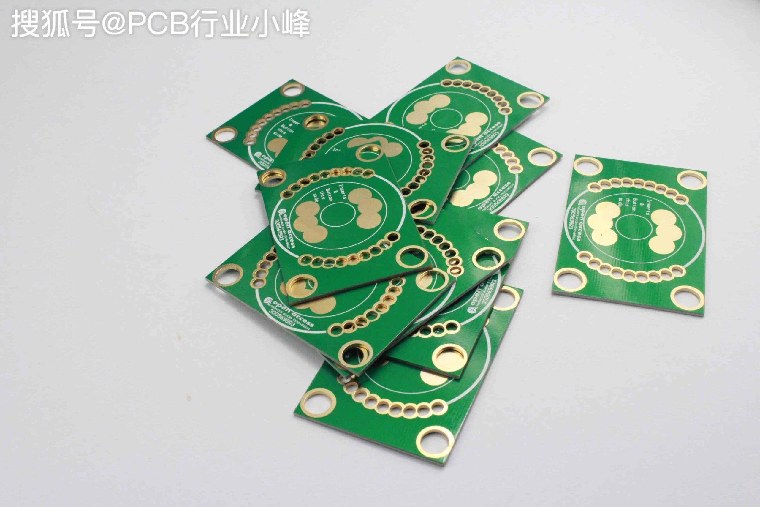
Printed circuit boards (PCBs) are the foundation of modern electronics. They provide the mechanical structure and electrical connections between components in electronic devices. There are several types of PCBs, each with their own characteristics and applications. The four main types of PCBs are:
1. Single-sided PCBs
Single-sided PCBs, as the name suggests, have the copper traces on only one side of the board. The components are mounted on the same side as the copper traces.
Advantages:
- Inexpensive to manufacture
- Simple layout and design
Disadvantages:
- Limited space for traces
- No traces on backside for heat dissipation or shielding
Applications:
- Simple electronic projects
- Low complexity circuits
- Cost-sensitive products
2. Double-sided PCBs
Double-sided PCBs have copper traces on both sides of the board with components mounted on either side. Traces and connectors on each side are connected by plated through-holes called vias.
Advantages:
- More space for complex circuit routing
- Traces on both sides improve heat dissipation
- Lower layer counts reduce costs
Disadvantages:
- More complex and expensive to manufacture than single-sided
- Limited in complexity compared to multilayer PCBs
Applications:
- Mid-complexity electronic products
- Cost-sensitive products needing more routing space
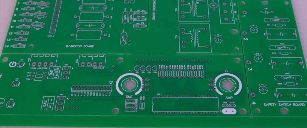
3. Multilayer PCBs
Multilayer PCBs consist of 4 or more conductive copper layers separated by insulating dielectric layers. Each layer can have traces, pads, and vias. Components are mounted on the outer layers.
Advantages:
- Very high component densities with traces on multiple layers
- Excellent for high-speed and high-frequency circuits
- Best EMI and noise shielding
Disadvantages:
- High design complexity
- Expensive to manufacture with more layers
Applications:
- Highly complex and dense digital circuits
- Cell phones, computers, automotive electronics
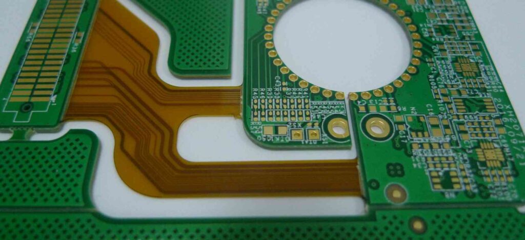
4. Flexible PCBs
Flexible PCBs use very thin, flexible substrate materials that allow the board to bend and flex. Common materials include polyimide and PEEK films.
Advantages:
- Can flex and bend to fit product enclosures
- Good for wearable electronics
- Withstands vibration and impact
Disadvantages:
- More expensive materials
- Limited in component densities
Applications:
- Wearable devices
- Implantable medical devices
- Consumer electronics needing flexing
Comparative Table of PCB Types
| PCB Type | Layers | Complexity | Cost | Key Characteristics |
|---|---|---|---|---|
| Single-Sided | 1 | Low | Low | – Least expensive <br>- Limited routing space |
| Double-Sided | 2 | Medium | Medium | – More routing than single-sided <br>- Improved heat dissipation |
| Multilayer | 4+ | High | High | – Very dense and complex routing <br>- Excellent EMI shielding |
| Flexible | 1-2 | Low/Medium | High | – Can flex and bend <br> – Good for wearables |
Choosing the Right PCB Type
When designing an electronic product, the PCB type should be selected based on factors like:
- Complexity – How complex are the circuits and routing? More layers allow for greater complexity.
- Space – Is component density and limited space a major concern? Multilayer PCBs excel here.
- Flexibility – Does the PCB need to flex and bend? Flex PCBs are required.
- EMI – Are radio interference and noise concerns? Multilayer PCBs provide the best shielding.
- Budget – What is the budget for the PCBs? Single-sided is cheapest while multilayer is most expensive.
- Quantity – Low volume prototype vs. high volume production will impact costs.
- Frequency – High frequency circuits demand controlled impedances like microstrips.
- Reliability – More layers improve shock/vibration reliability.
The PCB substrate material is also an important consideration. FR-4 glass epoxy is the most common and cost effective. High frequency boards may use RF materials like Rogers and ceramic substrates for very high frequency or thermal management.
PCB Design and Layout Guidelines
To leverage the full benefits of a PCB, it helps to follow design guidelines and best practices:
- Use adequate trace widths based on expected current. This prevents overheating.
- Manage impedance with controlled dimension traces for high speed signals.
- Use coplanar ground planes next to signal layers to control impedance.
- Use generous spacing between traces and pads to prevent shorts.
- Add generous thermal pads and vias underneath hot components.
- Use multiple vias when changing layers to reduce inductance.
- Separate analog and digital circuits to prevent noise coupling.
- Include bypass/decoupling capacitors near integrated circuits.
- Maximize use of each layer without overcrowding.
- Review design rules and stackup provided by PCB manufacturer.
PCB Manufacturing Process Overview
PCBs go through a complex, multi-step manufacturing process with strict quality control checks:
1. Design
- The PCB layout is designed in EDA software based on circuit schematics.
- Stackup, layer count, materials, finishes, and other parameters are defined.
- Output Gerber and drill files generated.
2. Fabrication Data Processing
- Gerber and drill files processed for manufacturing.
- Photomasks created.
- NC drill files generated.
3. Lamination
- Inner layers are fabricated by coating copper foil with photoresist.
- An image of the traces is transferred to the copper using photolithography.
- Etching removes unwanted copper, leaving behind the traces.
- Layers are laminated together using heat and pressure.
4. Through-hole Plating
- Holes are drilled through the PCB for vias and mounting holes.
- Walls are plated with copper to electrically connect layers.
5. Surface Finishes
- Outer layer traces coated with solder, gold, or other finish.
- Coatings protect traces from corrosion and provide solderability.
6. Solder Mask
- Entire PCB surface coated with epoxy, except areas needing solder.
- Prevents solder bridges between closely spaced traces.
7. Silkscreen
- Prints reference designators, symbols, warnings onto PCB.
8. Testing and Inspection
- Electrical testing checks for shorts, opens, and continuity.
- Automated optical inspection looks for defects.
- Impedance, propagation delay and other parameters measured.
This complex process ensures PCBs meet the design requirements and tolerances needed for functional products.
FQA
What are the key differences between single-sided and double-sided PCBs?
The main differences between single-sided and double-sided PCBs are:
- Single-sided have copper traces on only one side, while double-sided have traces on both sides.
- Double-sided allows for more complex routing with traces on both sides. Single-sided is limited in routing space.
- Double-sided is more expensive to fabricate but allows components on both sides. Single-sided has all components on one side.
- Double-sided has better heat dissipation and EMI shielding since it has a ground plane on the backside.
- Double-sided PCBs use plated through-hole vias to connect traces on both layers. These are not needed on single-sided.
- For simple circuits with low component density, single-sided PCBs are most cost effective. Double-sided are better for more complex routing.
How is impedance controlled in PCB traces?
Impedance is controlled in PCB traces through careful dimensioning and stackup design:
- Use traces with the correct width to achieve the desired impedance, usually 50-100 ohms.
- Keep trace widths consistent over the entire route to maintain impedance.
- Use a ground plane next to the signal layer to maintain constant impedance.
- Keep trace spaced far from the ground plane for higher impedance. Place near for lower.
- Use microstrip traces sandwiched between power and ground planes.
- Model the trace geometry and stackup in EDA tools to validate impedance.
- Specify differential pair trace spacing and widths for 100 ohm differential impedance.
- Avoid changes in layer stackup along trace routes to maintain consistent impedance.
What are the key advantages of multilayer PCBs?
Some key advantages of multilayer PCBs include:
- Extremely high component and circuit densities with multiple routing layers.
- Ability to segregate circuits types (analog, digital, RF) on different layers.
- Multiple ground planes for improved EMI shielding and noise isolation.
- Dense, controlled impedance routing for high speed signals.
- Small vias improve routing flexibility and reduce parasitic inductance.
- Power planes deliver clean, steady power distribution across the board.
- Heat dissipation routed internally between layers.
- Flexibility to optimize signal integrity, noise isolation, and density.
- More robust designs with interlayer connectors distributed through the PCB.
What are some best practices for PCB component placement?
Some best practices for component placement on PCB layouts include:
- Place decoupling capacitors as close as possible to IC power pins
- Group related components together instead of scattering them around
- Ensure adequate clearance between components to avoid shorts
- Keep high-speed traces as short and direct as possible
- Route signals orthogonally to reduce crosstalk when lines run in parallel
- Place connectors along board edges for easier cabling
- Ensure components fit within the board outline
- Distribute high-power components to avoid hotspots
- Place sensitive analog and digital circuits on separate PCB areas
- Ensure components are accessible for debugging and testing
- Follow manufacturer guidelines for component placement
- Verify components can be assembled by the pick-and-place machine
What are some common PCB substrate materials?
Some common materials used as the insulating substrate for PCBs include:
- FR-4 Glass Epoxy – Most common, cost effective material
- CEM-1 Cellulose Epoxy – Low cost, lower performance than FR-4
- FR-5 Glass Epoxy – High Tg and thermal performance
- GETEK – Paper-based phenolic resin, low cost
- Polyimide – Extremely high temperature resistance
- PTFE (Teflon) – Excellent high frequency material
- Rogers – High frequency circuit materials with good thermal conductivity
- Isola – Specialty laminates including high speed and RF materials
- Arlon – Microwave and thermal management substrates
- Taconic – RF materials with excellent stability
- Ceramic – Alumina or aluminum nitride for high frequency, high power
The substrate material is a key consideration and should be matched to the design requirements, operating frequency, power levels, and budget.


Leave a Reply