Introduction
A flex printed circuit board (PCB) is a type of printed circuit board that is flexible and can bend or flex. Flex PCBs consist of flexible dielectric substrate materials like polyimide that allow the board to flex and conform to different shapes without damage. They utilize conductive materials like copper to create the circuit traces and pads. Flex PCBs provide advantages over rigid PCBs including flexibility, space savings, and improved reliability in dynamic applications. This article will examine the key materials used in manufacturing flex PCBs and their properties.
Dielectric Substrate Materials
The dielectric substrate is the flexible insulating material that forms the base of the flex PCB. It provides mechanical support and electrical insulation between the conductive layers. Common substrate materials used include:
Polyimide
Polyimide film is the most common flexible dielectric used in flex PCBs. The two main types are:
- Kapton – Developed by DuPont, Kapton polyimide offers high heat resistance, chemical resistance, and mechanical strength. It has excellent electrical insulating properties.
- Upilex – An alternative polyimide film from Ube Industries noted for its extremely low thermal expansion.
Key properties:
- High mechanical flexibility and foldability
- Withstands high temperatures up to 400°C
- Chemically inert and resistant to most solvents
- Excellent electrical insulation properties
Polyester
Polyester films like PET provide an economical option but have lower maximum operating temperatures around 150°C. The relatively low glass transition temperature limits use in high temperature applications.
Liquid Crystal Polymer
LCP offers very high heat resistance up to 250°C and is resistant to humidity and chemicals. It has excellent electrical properties but is relatively expensive.
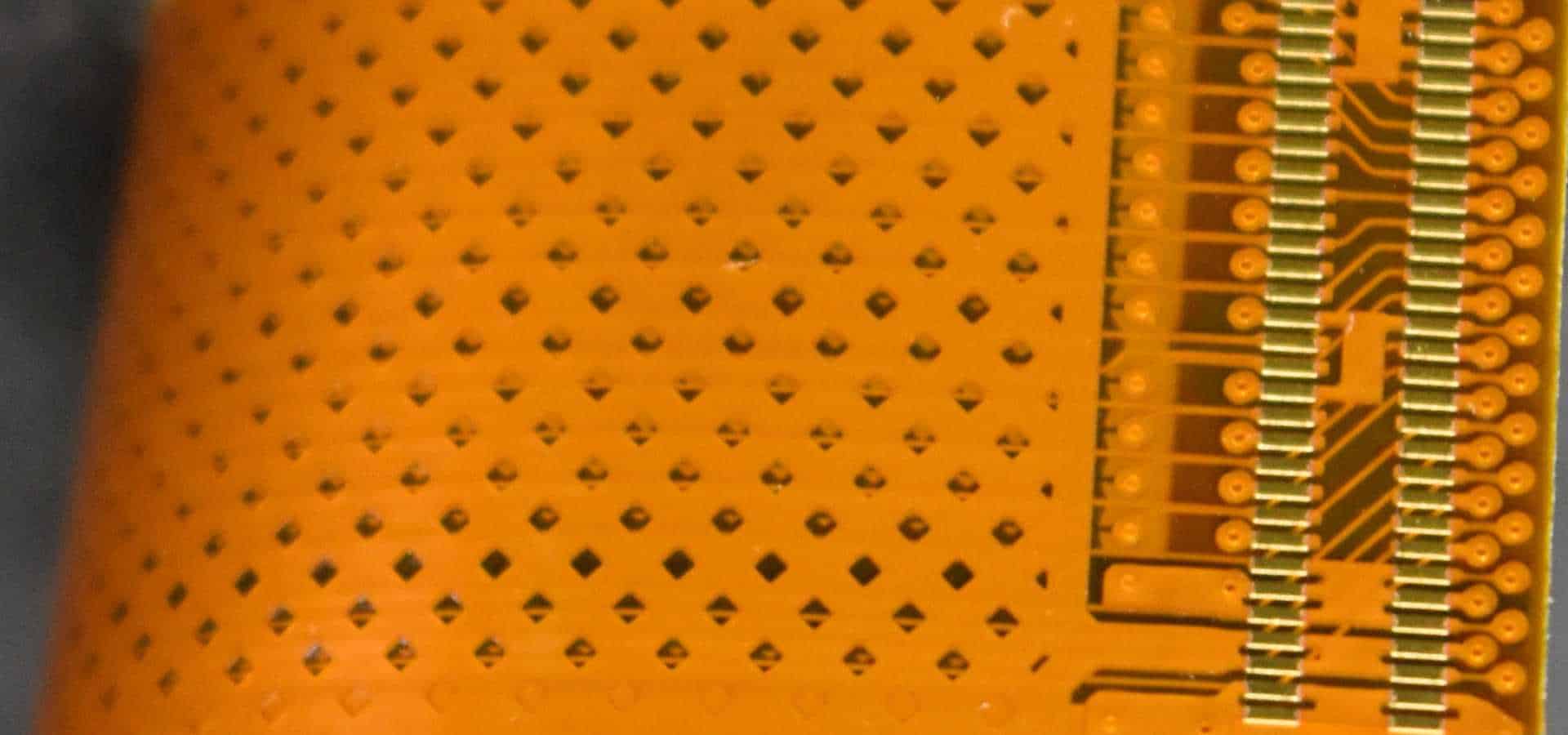
Conductive Materials
The conductive layers of traces, pads, and features are typically made from copper. Other options include:
Copper
- Most common conductive material used in PCBs due to high conductivity and low cost
- Rolled annealed copper with a very smooth surface finish
- Thickness ranges from 0.5 oz (17μm) to 2 oz (70μm) commonly
Aluminum
- Lower cost than copper but only about 60% of the conductivity
- Used when cost reduction is critical
Silver
- Highest conductivity of all metals but expensive
- Selected when high conductivity and performance required
Carbon nanotubes
- Emerging material that offers flexibility and high conductivity
- Still in R&D phase with challenges to overcome
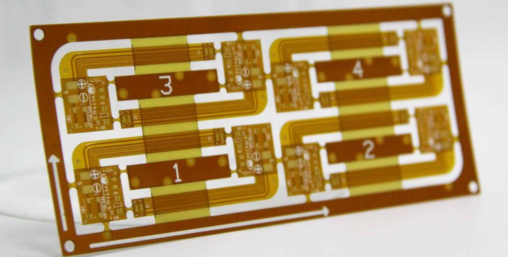
Coverlayers, Bondplies, and Adhesives
Additional flexible materials are used in multilayer flex PCB constructions for electrical insulation, bonding, and mechanical support:
Coverlayer
- Polyimide, polyester, or LCP film laminated over outer circuit layers
- Provides insulation and protects traces
Bondply
- Thin adhesive-coated dielectric films
- Bonds multiple circuit layers together in multilayer designs
Adhesives
- Acrylic or epoxy adhesive films
- Bond coverlayers and bondplies to circuit layers
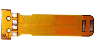
Common Flex PCB Constructions
There are two main constructions of flex PCBs – single layer and multilayer:
Single Layer
Consists of a single layer of copper traces on a flexible dielectric substrate. Simplest and least expensive.
Multilayer
Two or more circuit layers separated by flexible dielectric bondply layers. Allows for higher circuit density and complexity.
##Manufacturing Process
Flex PCBs follow a similar fabrication process to rigid PCBs. The main steps include:
- Substrate cleaning – Removes oils, dust, and debris
- Photolithography – Photoresist laminated, exposed, and developed to form circuit pattern
- Etching – Unwanted copper removed to form traces and pads
- Stripping – Residual photoresist removed
- Coverlayer lamination – Insulating coverlayer applied over traces
- Drilling – Holes drilled for vias and component mounts
- Plating – Copper-plated through holes and vias
- Solder mask – Covers exposed copper surfaces besides pads
- Finishing – Hot air solder leveling, immersion silver, or other surface finish
- Testing – Electrical testing to validate function
- Singulation – Individual boards cut from panel
Key Properties
Flex PCBs offer several advantageous properties:
- Flexibility – Can bend and flex repeatedly without damage
- Lightweight – Thin, lightweight circuit materials
- Durability – Withstands vibration, shock, and flexing
- Space savings – Conforms tightly to product contours
- Higher reliability – Dynamic flexing reduces stresses
- Lower assembly cost – Allows complex 3D assemblies
Applications
The unique properties of flex PCBs make them suitable for:
- Consumer electronics – Cell phones, laptops, tablets, wearables
- Automotive – Instrument clusters, engine electronics, sensors
- Industrial – Robotics, machine controls, test/measurement
- Medical – Patient monitoring, implants, imaging equipment
- Aerospace/military – Guidance systems, engine controls
Any application where size, weight, or reliability considerations are critical can benefit from flex PCB technology. The circuits can be folded, twisted, and bent to fit into tight spaces where rigid boards cannot.
Comparison to Rigid PCBs
| Parameter | Flex PCB | Rigid PCB |
|---|---|---|
| Dielectric substrate | Flexible polyimide, PET, LCP | Rigid FR-4,ceramic |
| Conductive material | Copper, aluminum, silver | Copper primary |
| Circuit layers | Single or multilayer | Up to 30+ layers |
| Max temperature | 130-400°C depending on dielectric | 130°C standard FR-4 |
| Flexibility | Can bend and flex repeatedly | Rigid, no flex |
| Weight | Extremely lightweight | Heavier than flex |
| Reliability | Very high, flexing reduces stresses | Good overall |
| Cost | Higher than rigid PCBs | Lower cost |
Frequently Asked Questions
What are the key benefits of using a flex PCB?
Flex PCBs provide several advantages over rigid boards including flexibility, reduced space requirements, lighter weight, improved reliability in dynamic environments, and simplified assembly. The ability to bend and conform the circuitry allows compact, efficient electronic designs.
What are some common applications of flex PCB technology?
Flex PCBs are widely used in consumer electronics, automotive electronics, industrial controls, medical equipment, robotics, aerospace systems, and military electronics. Any application where space, weight, or reliability considerations are important can benefit from flex circuits.
How many layers can you get on a flex PCB?
While rigid boards support many more layers, flex PCBs typically range from single layer to about 10 layers. Occasionally flex boards up to 20 layers are produced for highly complex designs. The flexing requirements and small bend radii place practical limits on the number of layers.
Can you solder components to a flex PCB?
Yes, surface mount components can be soldered to the pads and traces on the outer circuit layers of a flex PCB, similar to rigid PCB assembly. Care must be taken in handling to avoid cracking solder joints when flexing. Adhesives or clips may be used to relieve stresses on components.
Are flex PCBs more expensive than rigid PCBs?
Generally flex PCBs have a higher cost per square inch compared to rigid boards. The flexible substrate materials and specialized processing increase the fabrication costs over standard rigid PCBs. However, the system-level savings can offset the higher initial cost.


Leave a Reply