Introduction to PCB-UV-Lasers
Printed Circuit Boards (PCBs) are the backbone of modern electronics, found in virtually every electronic device we use today. The manufacturing process of PCBs has evolved significantly over the years, with new technologies emerging to improve efficiency, precision, and quality. One such technology is the use of ultraviolet (UV) lasers in PCB manufacturing.
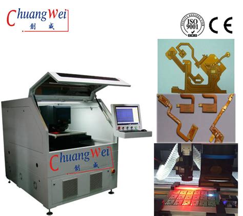
UV lasers have become increasingly popular in the PCB industry due to their ability to precisely cut, drill, and engrave various materials used in PCB fabrication. These lasers operate in the ultraviolet spectrum, typically with wavelengths between 355 and 375 nanometers. The shorter wavelength of UV lasers allows for higher precision and smaller feature sizes compared to traditional infrared (IR) lasers.
Advantages of UV Lasers in PCB Manufacturing
- High precision: UV lasers can achieve feature sizes as small as 25 microns, enabling the creation of high-density interconnects (HDI) and micro-via drilling.
- Minimal thermal damage: The short pulse duration and high energy density of UV lasers minimize heat-affected zones (HAZ), reducing thermal damage to the surrounding material.
- Versatility: UV lasers can process a wide range of materials, including copper, polyimide, and glass-reinforced epoxy (FR-4).
- Increased efficiency: UV lasers offer faster processing speeds and reduced cycle times compared to traditional mechanical drilling methods.
Applications of PCB-UV-Lasers
Micro-Via Drilling
One of the primary applications of UV lasers in PCB manufacturing is micro-via drilling. Micro-vias are small, laser-drilled holes that connect layers within a multi-layer PCB. These vias are essential for creating high-density interconnects and enabling the miniaturization of electronic devices.
UV lasers are particularly well-suited for micro-via drilling due to their high precision and minimal thermal damage. The laser beam can be focused to a spot size as small as 25 microns, allowing for the creation of micro-vias with diameters ranging from 50 to 150 microns. Additionally, the short pulse duration of UV lasers minimizes the heat-affected zone, reducing the risk of delamination or other thermal-related defects.
| Via Type | Diameter Range (microns) | Depth Range (microns) |
|---|---|---|
| Standard | 200 – 500 | 100 – 500 |
| Micro | 50 – 150 | 25 – 150 |
Blind and Buried Via Formation
UV lasers are also used for the formation of blind and buried vias in multi-layer PCBs. Blind vias connect an outer layer to an inner layer, while buried vias connect two or more inner layers without reaching the outer layers.
The process of creating blind and buried vias involves laser drilling from one side of the PCB to a specific depth, stopping at the desired layer. UV lasers offer precise depth control, enabling the formation of these vias without damaging adjacent layers. This precision is crucial for maintaining the integrity of the PCB and ensuring reliable electrical connections.
PCB Patterning and Cutting
In addition to via formation, UV lasers are used for PCB patterning and cutting. Laser patterning involves the selective removal of copper or other conductive materials to create the desired circuit pattern on the PCB. UV lasers can achieve fine feature sizes and precise geometries, enabling the creation of high-density circuit patterns.
UV lasers are also used for cutting PCBs into their final shapes. Compared to mechanical cutting methods, laser cutting offers several advantages, including:
- Reduced mechanical stress on the PCB
- Minimal debris and contamination
- Faster cutting speeds
- Ability to create complex shapes and cutouts
Solder Mask Removal
Solder masks are insulating layers applied to the surface of a PCB to protect the copper traces and prevent short circuits. In some cases, it is necessary to remove the solder mask selectively to expose specific areas for component placement or electrical testing.
UV lasers can be used for selective solder mask removal, offering precise control over the area to be exposed. The high energy density of UV lasers allows for the removal of the solder mask without damaging the underlying copper traces. This process is faster and more accurate than traditional chemical etching methods.

Laser Systems for PCB Manufacturing
Several types of laser systems are used in PCB manufacturing, each with its own advantages and applications.
Nanosecond UV Lasers
Nanosecond UV lasers, such as Nd:YAG lasers with third harmonic generation (355 nm), are commonly used for micro-via drilling and PCB patterning. These lasers offer pulse durations in the nanosecond range, providing a balance between precision and processing speed.
Advantages of nanosecond UV lasers include:
- High peak power for efficient material removal
- Relatively low cost compared to picosecond and femtosecond lasers
- Proven reliability in industrial settings
Picosecond UV Lasers
Picosecond UV lasers offer even shorter pulse durations, typically in the range of 10 to 100 picoseconds. These lasers provide higher precision and smaller feature sizes compared to nanosecond lasers.
Advantages of picosecond UV lasers include:
- Minimal heat-affected zones and thermal damage
- Ability to create smaller vias and finer circuit patterns
- Improved edge quality and reduced debris
Femtosecond UV Lasers
Femtosecond UV lasers represent the cutting edge of laser technology, with pulse durations in the femtosecond range (10^-15 seconds). These lasers offer the highest precision and minimal thermal effects.
Advantages of femtosecond UV lasers include:
- Virtually no heat-affected zones
- Ability to process delicate materials without thermal damage
- Highest precision and smallest feature sizes
However, femtosecond lasers are more expensive and complex than nanosecond and picosecond lasers, limiting their widespread adoption in PCB manufacturing.

Integrating UV Lasers into PCB Manufacturing Processes
To effectively integrate UV lasers into PCB manufacturing processes, several factors must be considered:
- Laser system selection: Choose a laser system that offers the required precision, processing speed, and compatibility with the materials used in your PCB manufacturing process.
- Process optimization: Develop and optimize laser processing parameters, such as pulse energy, repetition rate, and scanning speed, to achieve the desired results consistently.
- Automation and control: Integrate the laser system with automated handling and control systems to ensure efficient and accurate processing of large quantities of PCBs.
- Safety considerations: Implement appropriate safety measures, such as protective enclosures and eye protection, to ensure the safe operation of UV laser systems.

Future Trends and Developments
As the demand for smaller, more complex electronic devices continues to grow, the use of UV lasers in PCB manufacturing is expected to increase. Future trends and developments in this field may include:
- Increased adoption of picosecond and femtosecond lasers for ultra-high precision applications
- Development of new laser-compatible materials for PCB fabrication
- Integration of artificial intelligence and machine learning algorithms for process optimization and quality control
- Advancements in laser system miniaturization and cost reduction
Frequently Asked Questions (FAQ)
1. What are the main advantages of using UV lasers in PCB manufacturing?
UV lasers offer several advantages in PCB manufacturing, including high precision, minimal thermal damage, versatility in processing different materials, and increased efficiency compared to traditional methods.
2. What is the difference between nanosecond, picosecond, and femtosecond UV lasers?
The main difference between these laser types is their pulse duration. Nanosecond lasers have pulse durations in the nanosecond range (10^-9 seconds), picosecond lasers in the picosecond range (10^-12 seconds), and femtosecond lasers in the femtosecond range (10^-15 seconds). Shorter pulse durations generally offer higher precision and reduced thermal effects.
3. Can UV lasers be used for both rigid and flexible PCBs?
Yes, UV lasers can be used for both rigid and flexible PCBs. The high precision and minimal thermal damage of UV lasers make them suitable for processing a wide range of PCB materials, including flexible substrates like polyimide.
4. How does the use of UV lasers impact the overall cost of PCB manufacturing?
While the initial investment in UV laser systems can be higher than traditional manufacturing methods, the increased efficiency, precision, and reduced processing time can lead to overall cost savings in the long run. Additionally, the ability to create high-density interconnects and smaller feature sizes can enable the production of more advanced and valuable PCB designs.
5. What safety measures should be implemented when using UV lasers in PCB manufacturing?
When using UV lasers in PCB manufacturing, it is crucial to implement appropriate safety measures. These include the use of protective enclosures to contain laser radiation, eye protection for operators, and strict adherence to laser safety protocols. Proper training and safety procedures should be in place to ensure the safe operation of UV laser systems.
Conclusion
The use of UV lasers in PCB manufacturing has revolutionized the industry, enabling the production of high-density, high-precision circuit boards with minimal thermal damage. From micro-via drilling and blind and buried via formation to PCB patterning and cutting, UV lasers offer a versatile and efficient solution for modern PCB fabrication.
As the electronics industry continues to push the boundaries of miniaturization and performance, the adoption of UV laser technology in PCB manufacturing is expected to grow. By understanding the advantages, applications, and future trends of PCB-UV-lasers, manufacturers can stay at the forefront of this exciting field and deliver the next generation of advanced electronic devices.


Leave a Reply