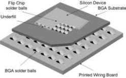
Introduction to BGA Soldering
Ball Grid Array (BGA) is a surface-mount packaging used for integrated circuits. BGA packages are used to permanently mount devices such as microprocessors. A BGA can provide more interconnection pins than can be put on a dual in-line or flat package. The whole bottom surface of the device can be used, instead of just the perimeter.
Advantages of BGA Packages
- Smaller package footprint compared to other SMT packages
- Higher lead/pin density and hence increased connectivity
- Lower thermal resistance between the package and PCB
- Better electrical performance due to shorter distance between package and PCB
Common BGA Soldering Defects
Despite the advantages, BGAs have their own set of challenges when it comes to soldering. Here are some of the most common BGA soldering defects:
1. Bridging
Bridging occurs when solder paste connects adjacent solder balls causing a short circuit. This can happen due to:
– Excessive solder paste deposit
– Poor paste printing
– Component misalignment
– Inappropriate reflow profile
2. Open Connection/Solder Joint
An open connection happens when there is insufficient solder to form a proper joint between the package ball and PCB pad. Causes include:
– Insufficient solder paste deposit
– Poor wetting of solder paste to pad or ball
– Inappropriate reflow profile
– Contamination preventing solder flow
3. Head-in-Pillow (HiP)
In a head-in-pillow defect, the solder paste wets the PCB pad but not the package ball, resulting in a partial connection. Main drivers are:
– Oxide buildup on package balls
– Warpage of package or board
– Inappropriate reflow profile
4. Solder Voids
Solder voids are cavities formed within the solder joint. While some voiding is common and acceptable, excessive voiding can weaken the joint. Factors contributing to voids include:
– Solder paste formulation
– Reflow profile – inadequate time above liquidus
– Surface finish and contamination
5. Black Pad Syndrome
Black pad syndrome results in weak and brittle solder joints due to a reaction between the PCB electroless nickel/immersion gold (ENIG) surface finish and phosphorus from the electroless nickel bath. This is a PCB manufacturing issue rather than an assembly problem.

Preventing BGA Soldering Defects
Careful process design and control are essential to minimize BGA soldering defects. Key considerations include:
1. Solder Paste Printing
- Use a stencil with appropriate aperture size and shape for the BGA
- Ensure proper stencil alignment and gasketing
- Control paste viscosity, print speed, pressure, and separation speed
- Inspect paste deposits for consistent volume and shape
2. Component Placement
- Ensure accurate component positioning, both laterally and rotationally
- Minimize package warpage through proper storage and handling
- Use a placement machine with good accuracy and repeatability
3. Reflow Soldering
- Develop a reflow profile suitable for the solder paste and components
- Ensure the profile reaches adequate peak temperature and time above liquidus
- Minimize temperature gradients and thermal shock
- Control cooling rate to prevent excessive intermetallic growth
4. PCB Design and Surface Finish
- Design pad sizes and shapes to maximize solder joint strength
- Specify a suitable PCB surface finish, typically OSP, ENIG, or ImAg
- Control surface finish thickness and quality
- Minimize PCB Warpage through proper material selection and design

Inspecting and Testing BGA Solder Joints
Assessing BGA solder joint quality can be challenging since the joints are hidden under the package. Methods include:
1. X-Ray Inspection
X-ray is the most common method for inspecting BGA solder joints. It allows detection of bridging, opens, voids, and other defects. However, x-ray cannot detect all defect types and requires skilled interpretation.
2. Endoscopic Inspection
An endoscope or borescope can be used to visually inspect the outer rows of solder balls. This method is limited to the visible balls and cannot detect internal defects.
3. Automated Optical Inspection (AOI)
AOI systems can check for missing or misaligned components and measure the amount of solder paste before reflow. However, post-reflow inspection is limited to the outer rows of balls.
4. Electrical Testing
Various electrical tests, such as in-circuit test (ICT), flying probe test, and boundary scan test, can verify connectivity and detect opens and shorts. Electrical tests do not provide information about joint shape or microstructure.
5. Dye and Pry
The dye and pry method involves applying a penetrant dye, prying off the BGA, and inspecting the dyed area to assess joint shape and wetting. This destructive technique is used for failure analysis, not production testing.

Reworking BGA Solder Joints
If a defective BGA solder joint is identified, it may be possible to rework the joint without replacing the entire board. The basic steps are:
- Remove the defective component using hot air or infrared heating
- Clean the site of old solder and residue
- Apply new solder paste or flux
- Place a new component and reflow
- Clean and inspect the reworked joint
Successful BGA rework requires precise temperature control, proper tools, and skilled operators. Rework should be minimized through effective process control.
Conclusion
BGA packages offer many advantages but also present challenges for PCB assembly. Understanding the common defect types, their causes, and prevention methods is essential for achieving high yield and reliability. Effective process design, control, and monitoring can minimize BGA soldering defects. When defects do occur, careful inspection and rework can salvage boards and avoid costly scrap.
Frequently Asked Questions (FAQ)
1. What is the most common BGA soldering defect?
According to industry studies, the most common BGA soldering defects are opens (insufficient solder joint), shorts (bridging between adjacent balls), and voids (cavities within the solder joint).
2. Can you X-ray BGA solder joints?
Yes, X-ray inspection is the most widely used method for assessing BGA solder joint quality. X-ray allows detection of defects such as bridging, opens, and voids that are hidden under the component. However, X-ray has limitations and requires skilled interpretation.
3. What causes head-in-pillow BGA defects?
Head-in-pillow defects occur when the solder paste wets the PCB pad but not the component ball, resulting in a partial connection. The main causes are oxide buildup on the component balls, warpage of the component or board, and an inappropriate reflow profile that fails to fully collapse the ball onto the paste.
4. How can I prevent BGA bridging?
To prevent BGA solder bridging, use a stencil with appropriate aperture size and shape for the paste deposit, ensure good stencil gasketing and alignment, control paste print parameters for consistent deposits, place components accurately, and use a reflow profile that fully melts the paste without excessive flow.
5. Can a defective BGA be reworked?
In many cases, a defective BGA solder joint can be reworked by removing the component, cleaning the site, applying new paste or flux, placing a new component, and reflowing. Successful rework requires precise temperature control, proper tools, and skilled operators. However, rework introduces additional thermal stress and should be minimized through good initial process control.
| Defect Type | Causes | Prevention |
|---|---|---|
| Bridging | – Excessive solder paste – Poor paste printing – Component misalignment – Inappropriate reflow |
– Proper stencil design – Print parameter control – Accurate component placement – Optimized reflow profile |
| Open | – Insufficient solder paste – Poor wetting – Inappropriate reflow – Contamination |
– Adequate paste volume – Proper surface finish – Optimized reflow profile – Cleanliness |
| Head-in-Pillow | – Oxide on balls – Component/board warpage – Inappropriate reflow |
– Ball surface preparation – Warpage control – Optimized reflow profile |
| Solder Voids | – Paste formulation – Inadequate reflow – Surface contamination |
– Suitable paste selection – Reflow profile optimization – Surface cleanliness |


Leave a Reply