Understanding the Basics of PCB Design
What is a PCB?
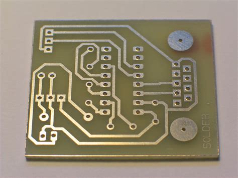
A PCB is a flat board made of insulating material, such as fiberglass or plastic, with conductive tracks, pads, and other features etched onto its surface. It serves as a base for connecting electronic components using conductive pathways, tracks, or signal traces.
Types of PCBs
PCBs can be classified into different types based on their construction and the number of layers:
| Type | Description |
|---|---|
| Single-layer PCB | Has conductive tracks on one side of the board |
| Double-layer PCB | Has conductive tracks on both sides of the board |
| Multi-layer PCB | Has multiple layers of conductive tracks sandwiched between insulating layers |
PCB Design Software
To design a PCB, you need specialized software that allows you to create schematic diagrams, layout the components, and generate manufacturing files. Some popular PCB design software include:
- Altium Designer
- KiCad
- Eagle
- OrCAD
- Autodesk EAGLE
Planning Your PCB Design
Define Your Requirements
Before starting your PCB design, clearly define your requirements:
- Purpose of the PCB
- Required functionality
- Size and shape constraints
- Environmental factors (temperature, humidity, etc.)
- Budget and timeline
Create a Schematic Diagram
A schematic diagram is a visual representation of your circuit’s components and their interconnections. It helps you plan the logical layout of your PCB. Consider the following when creating your schematic:
- Use standard symbols for components
- Label components and nets clearly
- Group related components together
- Use hierarchical design for complex circuits
Component Selection
Choosing the right components is crucial for the success of your PCB design. Consider the following factors when selecting components:
- Functionality and specifications
- Package type and size
- Availability and cost
- Manufacturer reputation and support

PCB Layout Considerations
Component Placement
Proper component placement is essential for optimizing the PCB’s performance and manufacturability. Keep these points in mind:
- Place components logically based on their function
- Minimize the distance between related components
- Consider the component’s orientation for ease of assembly
- Leave sufficient space for routing and manufacturing
Routing and Trace Width
Routing is the process of creating conductive paths between components on the PCB. Consider the following when routing your PCB:
- Use appropriate trace widths based on the current carrying capacity
- Maintain consistent trace widths and spacing
- Avoid sharp angles and use rounded corners
- Use ground planes for better signal integrity and EMI reduction
Power and Ground Management
Proper power and ground management is crucial for the stability and reliability of your PCB. Consider the following:
- Use dedicated power and ground planes
- Decouple power supplies with capacitors near the components
- Use star or grid topology for power distribution
- Avoid creating ground loops
Signal Integrity and EMI Reduction
Signal integrity and electromagnetic interference (EMI) are critical aspects of PCB design. To ensure optimal signal quality and reduce EMI:
- Use appropriate routing techniques, such as differential pairs and controlled impedance
- Minimize crosstalk by proper spacing and shielding
- Use ground planes and stitching vias to reduce EMI
- Follow high-speed design guidelines for critical signals

Manufacturing and Assembly Considerations
PCB Fabrication
When designing your PCB, keep the manufacturing process in mind:
- Choose the appropriate PCB material based on your requirements
- Specify the copper thickness and trace width based on the current carrying capacity
- Define the minimum hole size and spacing based on the manufacturer’s capabilities
- Provide clear and complete manufacturing files (Gerber, drill files, etc.)
PCB Assembly
Consider the following aspects for smooth PCB assembly:
- Choose components with compatible package types and sizes
- Provide clear and accurate assembly instructions
- Use appropriate solder mask and silkscreen for component identification
- Consider the assembly process (manual, SMT, or mixed) and its limitations

Testing and Verification
Design Rule Check (DRC)
Before sending your PCB design for manufacturing, perform a thorough Design Rule Check (DRC) to ensure it meets the manufacturer’s specifications and design guidelines. DRC helps identify issues such as:
- Minimum trace width and spacing violations
- Incomplete or missing connections
- Overlapping components or traces
- Incorrect hole sizes or spacing
Prototyping and Testing
Once your PCB is manufactured, it’s essential to prototype and test it thoroughly:
- Visually inspect the PCB for any manufacturing defects
- Perform continuity tests to verify proper connections
- Test the functionality of the PCB under different operating conditions
- Validate the PCB’s performance against the design requirements
Frequently Asked Questions (FAQ)
-
What is the difference between a schematic and a PCB layout?
A schematic is a logical representation of the circuit, showing the components and their connections. A PCB layout, on the other hand, is the physical representation of the circuit on the PCB, showing the actual placement of components and routing of traces. -
How do I choose the right PCB material for my design?
The choice of PCB material depends on factors such as the operating environment, frequency, and cost. Common PCB materials include FR-4, Rogers, and polyimide. Consult with your PCB manufacturer and consider your specific requirements to select the most suitable material. -
What is the importance of decoupling capacitors in PCB design?
Decoupling capacitors are used to reduce noise and stabilize the power supply to individual components. They are placed close to the power pins of ICs to provide a local reservoir of charge and minimize the effect of voltage fluctuations caused by switching activities. -
How can I minimize crosstalk in my PCB design?
Crosstalk can be minimized by proper trace routing, spacing, and shielding. Some techniques include: - Keeping sensitive traces away from noisy traces
- Using ground planes between layers to provide shielding
- Increasing the spacing between traces
-
Using differential signaling for critical signals
-
What are the common file formats used for PCB manufacturing?
The most common file formats used for PCB manufacturing are Gerber files (RS-274X) and drill files (Excellon). Gerber files contain information about the copper layers, solder mask, silkscreen, and other features of the PCB. Drill files specify the location, size, and type of holes required for the PCB.
Conclusion
PCB design is a complex process that requires careful planning, attention to detail, and adherence to best practices. By understanding the basics of PCB design, planning your design carefully, considering layout and manufacturing aspects, and thoroughly testing your PCB, you can create reliable and efficient electronic circuits.
Remember to keep up with the latest industry trends, consult with experienced designers, and continuously improve your skills. With practice and perseverance, you can master the art of PCB design and bring your electronic ideas to life.


Leave a Reply