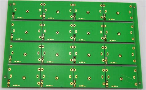
What is a Double-sided PCB?
A double-sided PCB, also known as a double-layer or two-layer PCB, is a printed circuit board with conductive copper layers on both sides of the insulating substrate. This allows for a higher density of components and interconnections compared to single-sided PCBs. Double-sided PCBs are widely used in electronic devices, from consumer electronics to industrial applications, due to their increased functionality and compact size.
Advantages of Double-Sided PCBs
- Higher component density
- Improved signal integrity
- Better power distribution
- Compact size
- Cost-effective for medium-complexity designs
Structure of a Double-Sided PCB
A double-sided PCB consists of several layers:
- Top copper layer
- Insulating substrate
- Bottom copper layer
- Solder mask (top and bottom)
- Silkscreen (top and bottom)
Top and Bottom Copper Layers
The top and bottom copper layers are the conductive surfaces where components are mounted and interconnected. These layers are typically made of copper foil, which is laminated onto the insulating substrate. The thickness of the copper foil is usually measured in ounces per square foot (oz/ft²). Common thicknesses include:
| Copper Weight (oz/ft²) | Thickness (mm) |
|---|---|
| 0.5 | 0.0175 |
| 1 | 0.0350 |
| 2 | 0.0700 |
The copper layers are etched to create the desired circuit patterns, which include traces, pads, and vias.
Insulating Substrate
The insulating substrate is the core material of the PCB, providing mechanical support and electrical insulation between the copper layers. The most common substrate material is FR-4, a glass-reinforced epoxy laminate. Other substrate materials include:
- CEM-1 (composite epoxy material)
- CEM-3 (composite epoxy material with higher glass content)
- Polyimide (high-temperature resistant)
- PTFE (low dielectric constant)
The thickness of the substrate depends on the application and the required mechanical strength. Typical thicknesses range from 0.4mm to 3.2mm.
Solder Mask
The solder mask is a protective coating applied to the copper layers, leaving only the exposed pads and vias for soldering. It prevents accidental short circuits and protects the copper traces from oxidation and damage. Solder masks are typically made of epoxy or acrylic materials and are available in various colors, with green being the most common.
Silkscreen
The silkscreen is a printed layer on top of the solder mask that provides text, logos, and component outlines for easy identification and assembly. It is typically white, but other colors are available. The silkscreen is usually made of epoxy or acrylic ink.

Materials Used in Double-Sided PCBs
Copper Foil
Copper foil is the most common conductive material used in PCBs due to its excellent electrical conductivity, thermal conductivity, and mechanical properties. The copper foil is typically electrodeposited (ED) or rolled annealed (RA).
- ED copper: Produced by electroplating, resulting in a smooth surface and uniform thickness. It has lower ductility and tensile strength compared to RA copper.
- RA copper: Produced by rolling and annealing, resulting in a matte surface and higher ductility and tensile strength compared to ED copper.
Insulating Substrates
FR-4
FR-4 is the most widely used insulating substrate in PCBs. It is a composite material made of woven fiberglass cloth impregnated with an epoxy resin. FR-4 has good mechanical, thermal, and electrical properties, making it suitable for a wide range of applications.
Properties of FR-4:
- Dielectric constant (Dk): 4.3-4.6 at 1 MHz
- Dissipation factor (Df): 0.02 at 1 MHz
- Thermal expansion coefficient (CTE): 12-16 ppm/°C
- Glass transition temperature (Tg): 130-140°C
- Flame retardant: Yes (UL 94 V-0)
Other Insulating Substrates
- CEM-1 and CEM-3: Composite epoxy materials with lower cost and performance compared to FR-4.
- Polyimide: High-temperature resistant substrate for applications that require operation above 150°C.
- PTFE: Low dielectric constant substrate for high-frequency applications, such as RF and microwave circuits.
Solder Mask Materials
Solder mask materials are typically epoxy or acrylic-based, with the following properties:
- Good adhesion to copper and substrate
- Resistance to solvents and chemicals
- High electrical insulation
- Flame retardant (UL 94 V-0)
- Available in various colors
Common solder mask materials include:
- Liquid photoimageable solder mask (LPISM): Applied as a liquid and patterned using photolithography.
- Dry film solder mask (DFSM): Applied as a dry film and patterned using photolithography.
Silkscreen Materials
Silkscreen materials are epoxy or acrylic-based inks that are screen printed onto the PCB. They have the following properties:
- Good adhesion to solder mask
- Resistance to solvents and chemicals
- High contrast for readability
- Available in various colors

Manufacturing Process of Double-Sided PCBs
The manufacturing process of double-sided PCBs involves several steps:
- Design and layout: The circuit schematic is created, and the PCB layout is designed using CAD software.
- CAM and tooling: The CAD files are converted into CAM (Computer-Aided Manufacturing) files, and tooling holes and alignment marks are added.
- Copper lamination: The copper foil is laminated onto both sides of the insulating substrate using heat and pressure.
- Drilling: Holes are drilled through the PCB for vias, component leads, and mounting.
- Copper plating: The drilled holes are plated with copper to create electrical connections between the top and bottom layers.
- Photolithography: The circuit pattern is transferred onto the copper layers using photoresist and UV light exposure.
- Etching: The unwanted copper is removed using a chemical etching process, leaving the desired circuit pattern.
- Solder mask application: The solder mask is applied and patterned using photolithography or screen printing.
- Surface finish: A surface finish, such as HASL (Hot Air Solder Leveling), ENIG (Electroless Nickel Immersion Gold), or OSP (Organic Solderability Preservative), is applied to the exposed copper pads to enhance solderability and protect against oxidation.
- Silkscreen printing: The silkscreen is printed onto the solder mask using screen printing.
- Electrical testing: The PCB is tested for shorts, opens, and other defects using automated optical inspection (AOI) and electrical testing equipment.
- Singulation: The individual PCBs are cut from the panel using routing or scoring.

Design Considerations for Double-Sided PCBs
When designing a double-sided PCB, several factors should be considered:
- Component placement: Place components strategically to minimize the length of traces and the number of vias required.
- Trace width and spacing: Ensure that the trace width and spacing are appropriate for the current carrying capacity and voltage requirements of the circuit.
- Via placement: Position vias to minimize the impact on signal integrity and to avoid interference with components and traces.
- Impedance control: For high-frequency or high-speed circuits, maintain consistent impedance along the traces to minimize signal reflections and distortions.
- Thermal management: Consider the thermal dissipation requirements of components and design the PCB layout accordingly, using techniques such as copper pours or thermal vias.
- EMI/EMC: Implement appropriate grounding and shielding techniques to minimize electromagnetic interference (EMI) and ensure electromagnetic compatibility (EMC).
- Manufacturing considerations: Adhere to the design rules and guidelines provided by the PCB manufacturer to ensure manufacturability and reliability.
Applications of Double-Sided PCBs
Double-sided PCBs are used in a wide range of electronic devices and applications, including:
- Consumer electronics: Smartphones, tablets, laptops, gaming consoles, and wearables.
- Automotive electronics: Engine control units, infotainment systems, and advanced driver assistance systems (ADAS).
- Industrial automation: Programmable logic controllers (PLCs), human-machine interfaces (HMIs), and sensors.
- Medical devices: Diagnostic equipment, patient monitoring systems, and implantable devices.
- Telecommunications: Routers, switches, and base stations.
- Aerospace and defense: Avionics, radar systems, and military communication equipment.
FAQ
1. What is the difference between a single-sided and a double-sided PCB?
A single-sided PCB has conductive copper on only one side of the insulating substrate, while a double-sided PCB has copper layers on both sides. Double-sided PCBs offer higher component density, improved signal integrity, and better power distribution compared to single-sided PCBs.
2. Can double-sided PCBs have through-hole components?
Yes, double-sided PCBs can accommodate both surface-mount and through-hole components. The through-hole components are inserted into drilled holes and soldered on both sides of the board.
3. What is the typical thickness of a double-sided PCB?
The thickness of a double-sided PCB depends on the substrate material and the application requirements. Typical thicknesses range from 0.4mm to 3.2mm, with 1.6mm being a common choice.
4. How are the top and bottom layers of a double-sided PCB connected?
The top and bottom layers of a double-sided PCB are connected through plated through-holes called vias. These vias are drilled and then plated with copper to create electrical connections between the layers.
5. What are the advantages of using a double-sided PCB over a single-sided PCB?
Double-sided PCBs offer several advantages over single-sided PCBs, including:
- Higher component density
- Improved signal integrity
- Better power distribution
- Compact size
- Cost-effective for medium-complexity designs
By utilizing both sides of the substrate, double-sided PCBs enable more complex circuits and designs in a smaller footprint, making them a popular choice for a wide range of electronic applications.


Leave a Reply