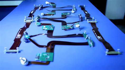
What are Flex Circuits?
Flex circuits are a type of printed circuit board (PCB) that consists of a thin, flexible substrate made of polyimide or other flexible materials. These substrates are laminated with copper traces and other components to create a functional electronic circuit. The flexibility of the substrate allows the circuit to be bent, folded, or twisted without damaging the components or connections.
Advantages of Flex Circuits
- Space-saving design
- Lightweight and thin
- High reliability and durability
- Resistance to vibration and shock
- Ability to conform to complex shapes
- Reduced assembly time and costs
Manufacturing Flex Circuits
The manufacturing process of flex circuits involves several steps, each requiring precision and expertise. Let’s take a closer look at each stage of the process.
Step 1: Design and Prototyping
The first step in manufacturing flex circuits is the design phase. Engineers use specialized software to create a detailed layout of the circuit, including the placement of components, traces, and vias. The design must take into account the intended use of the circuit, as well as any specific requirements for flexibility, durability, or performance.
Once the design is complete, a prototype is often created to test the functionality and reliability of the circuit. This prototype may be a small-scale version of the final product or a full-sized mock-up. Any necessary adjustments to the design are made based on the results of the prototype testing.
Step 2: Material Selection
The next step is to select the appropriate materials for the flex circuit. The most common substrate material is polyimide, which offers excellent thermal stability, chemical resistance, and mechanical strength. Other materials, such as polyester or liquid crystal polymer (LCP), may be used depending on the specific requirements of the application.
The copper foil used for the conductive traces is also carefully selected based on factors such as thickness, purity, and surface finish. Adhesives, cover layers, and other materials are chosen to ensure optimal performance and reliability.
Step 3: Substrate Preparation
Once the materials have been selected, the substrate is prepared for the lamination process. This involves cleaning the surface of the substrate to remove any contaminants or debris that could interfere with the adhesion of the copper foil.
In some cases, the substrate may be pre-treated with a chemical or plasma process to improve the bond strength between the substrate and the copper foil.
Step 4: Lamination
The lamination process involves bonding the copper foil to the substrate using heat and pressure. The copper foil is placed on top of the substrate, along with any necessary adhesives or bonding agents. The layered materials are then placed in a lamination press, where they are subjected to high temperatures and pressures to create a strong, permanent bond.
The lamination process must be carefully controlled to ensure uniform adhesion and to prevent any air bubbles or voids from forming between the layers.
Step 5: Etching
After lamination, the copper foil is selectively removed to create the desired circuit pattern. This is typically done using a photolithographic process, where a photoresist layer is applied to the copper foil and exposed to UV light through a patterned mask. The exposed areas of the photoresist are then developed and removed, leaving the copper foil exposed in the desired pattern.
The exposed copper is then etched away using a chemical solution, typically ferric chloride or ammonium persulfate. The etching process must be carefully controlled to ensure that the copper is completely removed in the desired areas, without over-etching or damaging the remaining copper traces.
Step 6: Drilling and Plating
After etching, any necessary holes or vias are drilled through the circuit board using a precision drill or laser. These holes are used to connect different layers of the circuit or to mount components.
The holes are then plated with a conductive material, typically copper, to create a continuous electrical connection between the layers. This is done using an electroplating process, where the circuit board is immersed in a plating solution and an electric current is applied to deposit the copper onto the walls of the holes.
Step 7: Solder Mask and Silkscreen
A solder mask layer is then applied to the surface of the circuit board to protect the copper traces from oxidation and to prevent accidental short circuits during the soldering process. The solder mask is typically a green or other colored polymer that is applied using a screen printing process.
A silkscreen layer is also often applied to the surface of the circuit board to add labels, logos, or other markings. This is done using a similar screen printing process, with a UV-curable ink.
Step 8: Surface Finishing
The final step in the manufacturing process is to apply a surface finish to the exposed copper traces and pads. This is done to protect the copper from oxidation and to improve the solderability of the circuit board.
Common surface finishes include:
- Hot Air Solder Leveling (HASL)
- Electroless Nickel Immersion Gold (ENIG)
- Immersion Silver
- Immersion Tin
- Organic Solderability Preservative (OSP)
The choice of surface finish depends on the specific requirements of the application, such as the type of components being used, the expected operating conditions, and the desired shelf life of the product.

Quality Control and Testing
Throughout the manufacturing process, strict quality control measures are in place to ensure that the flex circuits meet the required specifications and performance standards. This includes visual inspections, electrical testing, and environmental testing.
Visual inspections are performed at various stages of the process to check for any defects or irregularities in the circuit pattern, solder mask, or silkscreen. Automated optical inspection (AOI) systems are often used to quickly and accurately detect any issues.
Electrical testing is performed to verify the continuity and resistance of the copper traces and to ensure that there are no short circuits or open connections. This is typically done using a flying probe tester or a bed-of-nails tester.
Environmental testing may also be performed to ensure that the flex circuits can withstand the expected operating conditions, such as temperature extremes, humidity, vibration, or shock. This may involve subjecting the circuits to accelerated life testing or other simulated environmental conditions.

Applications of Flex Circuits
Flex circuits are used in a wide range of applications across various industries. Some common examples include:
Consumer Electronics
- Smartphones and tablets
- Wearable devices
- Digital cameras
- Gaming consoles
Medical Devices
- Implantable devices
- Diagnostic equipment
- Monitoring systems
- Surgical instruments
Automotive Electronics
- Engine control modules
- Sensor systems
- Infotainment systems
- Lighting systems
Aerospace and Defense
- Satellites and spacecraft
- Avionics systems
- Missile guidance systems
- Radar and communication systems
Industrial Automation
- Robotics and motion control
- Sensors and transducers
- Monitoring and control systems
- Telecommunications
Frequently Asked Questions (FAQ)
1. What is the typical thickness of a flex circuit?
Flex circuits can be manufactured in a wide range of thicknesses, depending on the specific requirements of the application. The thickness of the substrate material can range from 25 microns to 200 microns, while the overall thickness of the circuit, including the copper traces and any additional layers, can range from 50 microns to 500 microns or more.
2. What is the minimum feature size that can be achieved with flex circuits?
The minimum feature size that can be achieved with flex circuits depends on the specific manufacturing process and equipment being used. With standard photolithographic processes, the minimum trace width and spacing is typically around 50 microns. However, more advanced processes, such as laser direct imaging (LDI) or high-density interconnect (HDI) technology, can achieve feature sizes down to 25 microns or less.
3. What is the maximum number of layers that can be incorporated into a flex circuit?
The maximum number of layers that can be incorporated into a flex circuit depends on the specific design and manufacturing process being used. In general, flex circuits can be manufactured with up to 30 or more layers, although most applications typically require fewer than 10 layers. The number of layers is limited by factors such as the thickness of the substrate material, the required flexibility of the circuit, and the manufacturing costs.
4. What is the typical lead time for manufacturing flex circuits?
The lead time for manufacturing flex circuits can vary depending on the complexity of the design, the volume of the order, and the specific manufacturing processes and materials being used. In general, lead times can range from a few days to several weeks, depending on the specific requirements of the project. Rush orders or expedited services may be available for time-sensitive projects, but may come with additional costs or minimum order quantities.
5. How do the costs of flex circuits compare to traditional rigid PCBs?
In general, flex circuits tend to be more expensive than traditional rigid PCBs, due to the specialized materials, equipment, and processes required for their manufacture. The cost of a flex circuit can be several times higher than an equivalent rigid PCB, depending on factors such as the size, complexity, and volume of the order. However, the overall system cost may be lower with flex circuits due to their ability to simplify assembly, reduce weight and space requirements, and improve reliability and performance in demanding applications.
Flex circuits offer a unique combination of flexibility, durability, and performance that makes them an attractive option for a wide range of electronic applications. By understanding the manufacturing process and the key considerations involved in designing and producing flex circuits, engineers and product designers can take full advantage of this versatile technology to create innovative and reliable electronic products.
| Characteristic | Flex Circuits | Rigid PCBs |
|---|---|---|
| Thickness | 50-500 microns | 0.8-3.2 mm |
| Weight | Low | High |
| Flexibility | High | Low |
| Durability | High | Moderate |
| Cost | High | Moderate |
| Design Freedom | High | Moderate |
| Assembly | Simple | Complex |
Table 1: Comparison of flex circuits and rigid PCBs
| Industry | Applications |
|---|---|
| Consumer Electronics | Smartphones, wearables, digital cameras |
| Medical Devices | Implantable devices, diagnostic equipment |
| Automotive | Engine control modules, sensor systems |
| Aerospace | Satellites, avionics, radar systems |
| Industrial | Robotics, sensors, monitoring systems |
Table 2: Common applications of flex circuits by industry
The manufacturing of flex circuits is a complex and precise process that requires specialized materials, equipment, and expertise. By following a rigorous manufacturing process and implementing strict quality control measures, flex circuit manufacturers can produce high-quality, reliable circuits that meet the demanding requirements of a wide range of applications. As the demand for smaller, lighter, and more flexible electronic devices continues to grow, flex circuits will play an increasingly important role in shaping the future of the electronics industry.


Leave a Reply