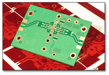
Introduction to PCB Prototyping
PCB (Printed Circuit Board) prototyping is a crucial step in the development of electronic products. It allows designers and engineers to test and validate their designs before mass production. PCB prototyping involves creating a physical copy of the PCB design, which can be used for testing, debugging, and optimization.
Benefits of PCB Prototyping
- Allows for early detection and correction of design flaws
- Enables testing of the PCB’s functionality and performance
- Provides a physical representation of the design for stakeholder feedback
- Reduces the risk of costly mistakes in mass production
The PCB CAM Process
The PCB CAM (Computer-Aided Manufacturing) process is an essential part of PCB prototyping. It involves using specialized software to convert the PCB design files into a format that can be used by manufacturing equipment.
Steps in the PCB CAM Process
- Design Import: The PCB design files (usually in Gerber or ODB++ format) are imported into the CAM software.
- Design Rule Check (DRC): The software checks the design for any violations of manufacturing constraints or design rules.
- Panelization: Multiple copies of the PCB design are arranged on a larger panel for efficient manufacturing.
- Tooling: Tooling holes and fiducial marks are added to the panel for alignment and registration during manufacturing.
- Output Generation: The final manufacturing files (usually in Gerber or Excellon format) are generated for use by the manufacturing equipment.
Importance of the PCB CAM Process
The PCB CAM process is critical for several reasons:
- Ensures Manufacturability: The CAM process checks the design for manufacturability and identifies any issues that could cause problems during production.
- Optimizes Production: Panelization and tooling optimize the use of materials and minimize waste, reducing production costs.
- Maintains Design Integrity: The CAM process ensures that the manufactured PCB matches the original design intent, without any unintended changes or distortions.

Choosing a PCB Prototyping Service
When selecting a PCB prototyping service, there are several factors to consider:
Technical Capabilities
- Supported PCB technologies (HDI, rigid-flex, etc.)
- Minimum feature sizes and tolerances
- Available materials and finishes
- Turnaround time and production capacity
Quality and Reliability
- Quality control processes and certifications (ISO, IPC, etc.)
- Track record and customer reviews
- Warranty and support policies
Cost and Value
- Pricing and volume discounts
- Additional services (assembly, testing, etc.)
- Shipping and logistics options

PCB Prototyping Case Studies
To illustrate the importance of PCB prototyping and the CAM process, let’s look at a few case studies.
Case Study 1: Medical Device Manufacturer
A medical device manufacturer was developing a new wearable health monitor. They used PCB prototyping to test and refine their design before moving to mass production. The CAM process identified several issues with the initial design, including incorrect hole sizes and spacing violations. By addressing these issues in the prototyping stage, the manufacturer avoided costly delays and rework in production.
Case Study 2: Automotive Electronics Supplier
An automotive electronics supplier was working on a new vehicle control module. They relied on PCB prototyping to validate the design’s performance under various environmental conditions (temperature, vibration, etc.). The CAM process optimized the panel layout to minimize material waste and reduce production costs. The successful prototyping phase allowed the supplier to meet their customer’s strict quality and reliability requirements.

Conclusion
PCB prototyping is an essential step in the development of electronic products, and the PCB CAM process plays a critical role in ensuring the success of prototyping efforts. By carefully selecting a PCB prototyping service and leveraging the capabilities of the CAM process, designers and engineers can create high-quality prototypes that meet their performance, reliability, and cost targets.
Frequently Asked Questions (FAQ)
1. How long does PCB prototyping usually take?
The turnaround time for PCB prototyping varies depending on the complexity of the design and the capabilities of the prototyping service. Simple designs can often be prototyped in a few days, while more complex designs may take several weeks.
2. What files are needed for PCB prototyping?
The specific files required for PCB prototyping may vary depending on the service provider, but generally include:
– Gerber files for each layer of the PCB
– Drill files specifying hole sizes and locations
– Fabrication drawings or assembly drawings
– Bill of Materials (BOM) for assembly services
3. What is the difference between PCB prototyping and mass production?
PCB prototyping typically involves smaller quantities (usually less than 100 pieces) and may use different manufacturing processes and materials compared to mass production. Prototyping is focused on validating the design and functionality, while mass production is optimized for volume, cost, and consistency.
4. Can PCB prototyping be used for complex designs like HDI or rigid-flex?
Yes, many PCB prototyping services offer advanced capabilities for complex designs. However, it’s important to carefully review the technical specifications and capabilities of the service provider to ensure they can meet the specific requirements of the design.
5. How much does PCB prototyping cost?
The cost of PCB prototyping depends on factors such as the size and complexity of the design, the number of layers, the quantity ordered, and any additional services (assembly, testing, etc.). Simple prototypes may cost a few hundred dollars, while complex designs can cost several thousand dollars. Many service providers offer online quoting tools to help estimate costs based on specific design parameters.


Leave a Reply