What is a PCB Stencil?
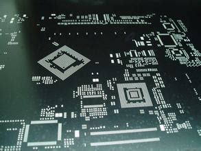
A PCB stencil, also known as a solder paste stencil, is a thin sheet of stainless steel or polyimide with laser-cut openings that correspond to the pads on a printed circuit board (PCB). The stencil is used to apply solder paste onto the PCB pads before components are placed and the board is sent through a reflow oven for soldering.
PCB stencils play a crucial role in the surface mount technology (SMT) assembly process, ensuring precise and consistent solder paste application. This leads to better solder joints, fewer defects, and higher yields in PCB manufacturing.
Why Use a PCB Stencil?
There are several reasons why PCB stencils are essential in the SMT assembly process:
-
Precision: PCB stencils allow for precise control over the amount and placement of solder paste on the PCB pads. This is especially important for fine-pitch components and high-density PCB designs.
-
Consistency: Using a stencil ensures that each PCB receives the same amount of solder paste on every pad, leading to consistent solder joints across the entire production run.
-
Efficiency: Stencil printing is a fast and efficient method for applying solder paste to multiple PCBs simultaneously, making it ideal for high-volume production.
-
Cost-effective: While there is an initial cost associated with creating a PCB stencil, the benefits of improved quality and reduced defects often outweigh the expense, especially for larger production runs.

Types of PCB Stencils
There are two main types of PCB stencils: stainless steel and polyimide.
Stainless Steel Stencils
Stainless steel stencils are the most common type used in PCB assembly. They are durable, long-lasting, and suitable for high-volume production. Key features of stainless steel stencils include:
- Thickness range: 0.1 mm to 0.2 mm (4 to 8 mils)
- Aperture size: As small as 0.1 mm (4 mils)
- Lifespan: 50,000 to 100,000 prints or more
Polyimide Stencils
Polyimide stencils, also known as plastic or polymer stencils, are a more flexible alternative to stainless steel. They are ideal for low-volume production or prototyping. Key features of polyimide stencils include:
- Thickness range: 0.05 mm to 0.13 mm (2 to 5 mils)
- Aperture size: As small as 0.2 mm (8 mils)
- Lifespan: 1,000 to 5,000 prints
| Feature | Stainless Steel Stencils | Polyimide Stencils |
|---|---|---|
| Thickness Range | 0.1 mm to 0.2 mm (4 to 8 mils) | 0.05 mm to 0.13 mm (2 to 5 mils) |
| Aperture Size | As small as 0.1 mm (4 mils) | As small as 0.2 mm (8 mils) |
| Lifespan | 50,000 to 100,000 prints or more | 1,000 to 5,000 prints |
| Durability | High | Moderate |
| Cost | Higher initial cost | Lower initial cost |
| Suitable for | High-volume production | Low-volume production, prototyping |

PCB Stencil Design Considerations
When designing a PCB stencil, several factors must be taken into account to ensure optimal solder paste application and PCB assembly results.
Aperture Size and Shape
The aperture size and shape in a PCB stencil should be carefully designed based on the PCB pad dimensions, component pitch, and solder paste properties. Generally, the aperture size should be slightly smaller than the pad size to prevent solder paste bridging between adjacent pads.
Common aperture shapes include:
- Rectangle: Most common shape, suitable for most SMD pads
- Circle: Used for round SMD pads or BGA solder balls
- Oblong: Combines rectangular and circular shapes, helpful for fine-pitch components
Stencil Thickness
The thickness of a PCB stencil determines the amount of solder paste deposited on the pads. Thicker stencils deposit more solder paste, while thinner stencils deposit less. The optimal stencil thickness depends on factors such as component size, pitch, and solder paste type.
Common stencil thicknesses for different component types:
| Component Type | Pitch | Stencil Thickness |
|---|---|---|
| Chip components | 0.5 mm to 1.27 mm | 0.1 mm to 0.15 mm |
| Fine-pitch QFPs | 0.4 mm to 0.8 mm | 0.1 mm to 0.12 mm |
| BGAs | 0.5 mm to 1.27 mm | 0.1 mm to 0.15 mm |
Aperture Wall Angle
The aperture wall angle, or sidewall angle, is the angle between the aperture wall and the stencil surface. A trapezoidal aperture shape with a wall angle between 1° to 5° is recommended to facilitate solder paste release and prevent clogging.
Fiducial Marks
Fiducial marks are reference points on the PCB and stencil that help align the stencil to the PCB during the solder paste printing process. It is crucial to include fiducial marks in both the PCB and stencil designs to ensure accurate alignment and prevent solder paste offset.

PCB Stencil Manufacturing Process
The PCB stencil manufacturing process typically involves the following steps:
-
Design: The stencil design is created based on the PCB layout and the specific requirements for solder paste application.
-
Material Selection: The appropriate stencil material (stainless steel or polyimide) is selected based on the production volume, durability requirements, and cost considerations.
-
Laser Cutting: The stencil design is transferred to the selected material, and a high-precision laser cuts the apertures according to the design.
-
Inspection: The finished stencil is inspected for accuracy, ensuring that all apertures are cut to the correct size, shape, and location.
-
Packaging: The stencil is packaged and shipped to the customer, ready for use in the solder paste printing process.
Solder Paste Printing Process
The solder paste printing process using a PCB stencil involves the following steps:
-
Stencil Alignment: The stencil is aligned to the PCB using the fiducial marks to ensure proper registration.
-
Solder Paste Application: Solder paste is placed on the stencil and spread across the surface using a squeegee blade, forcing the paste through the apertures and onto the PCB pads.
-
Stencil Removal: The stencil is carefully lifted away from the PCB, leaving the solder paste deposits on the pads.
-
Inspection: The PCB is inspected to ensure that the solder paste has been applied correctly, with no bridging, insufficient deposits, or other defects.
-
Component Placement: The PCB proceeds to the next step in the SMT assembly process, where components are placed on the solder paste deposits.
PCB Stencil Maintenance and Cleaning
Proper maintenance and cleaning of PCB stencils are essential to ensure consistent solder paste printing quality and extend the stencil’s lifespan.
Stencil Cleaning
Stencils should be cleaned regularly to remove solder paste residue and prevent clogging of the apertures. The cleaning frequency depends on factors such as the solder paste type, printing volume, and environment.
Common stencil cleaning methods include:
- Manual cleaning with solvents and wipes
- Automated stencil cleaning systems using ultrasonic, spray, or blasting technologies
Stencil Storage
When not in use, PCB stencils should be stored properly to prevent damage and contamination. Store stencils in a clean, dry environment, away from direct sunlight and extreme temperatures. Use protective covers or containers to prevent scratches and dents.
Frequently Asked Questions (FAQ)
-
What is the difference between a PCB stencil and a solder paste screen?
A PCB stencil and a solder paste screen serve the same purpose of applying solder paste to PCB pads. However, a stencil is typically made of stainless steel or polyimide and has laser-cut apertures, while a screen is made of a fine mesh with a stencil-like pattern applied to it. Stencils are more common in modern PCB assembly due to their higher precision and durability. -
Can I reuse a PCB stencil for different PCB designs?
No, a PCB stencil is specific to a particular PCB design. The apertures in the stencil are cut to match the pads on the PCB, so using the same stencil for a different PCB design would result in incorrect solder paste application. -
How long does a PCB stencil last?
The lifespan of a PCB stencil depends on the material and the printing volume. Stainless steel stencils can last for 50,000 to 100,000 prints or more, while polyimide stencils typically last for 1,000 to 5,000 prints. -
What is the optimal PCB stencil thickness?
The optimal PCB stencil thickness depends on factors such as the component size, pitch, and solder paste type. Generally, stencil thicknesses range from 0.1 mm to 0.2 mm (4 to 8 mils) for stainless steel and 0.05 mm to 0.13 mm (2 to 5 mils) for polyimide stencils. -
How often should I clean my PCB stencil?
The cleaning frequency for a PCB stencil depends on the solder paste type, printing volume, and environment. As a general rule, stencils should be cleaned every 4 to 8 hours of continuous printing or whenever print quality starts to degrade. Regular cleaning helps prevent solder paste buildup and ensures consistent print quality.
Conclusion
PCB stencils are an essential tool in the SMT assembly process, enabling precise and consistent solder paste application on PCB pads. By understanding the types, design considerations, manufacturing process, and maintenance requirements of PCB stencils, you can optimize your PCB assembly process and achieve higher quality solder joints and better yields.
When selecting a PCB stencil, consider factors such as production volume, component types, and solder paste properties to determine the best material, thickness, and aperture design for your specific application. Regular cleaning and proper storage of your stencils will help extend their lifespan and maintain consistent print quality.
By following the guidelines and best practices outlined in this guide, you can effectively incorporate PCB stencils into your SMT assembly process and take your PCB manufacturing to the next level.


Leave a Reply