What is Solderability Testing?
Solderability testing is a process used to evaluate the ability of electronic components and printed circuit boards (PCBs) to be soldered effectively. It assesses the wettability and adhesion properties of the surfaces to be soldered, ensuring reliable electrical connections and mechanical strength. Solderability testing is crucial in the electronics manufacturing industry to prevent soldering defects, improve product quality, and enhance the overall reliability of electronic assemblies.
Why is Solderability Testing Important?
Solderability testing plays a vital role in the electronics industry for several reasons:
-
Quality Assurance: Solderability testing helps identify components or PCBs that may have poor solderability due to factors such as contamination, oxidation, or improper storage conditions. By detecting these issues early, manufacturers can avoid using substandard components that could lead to soldering defects and product failures.
-
Process Optimization: The results of solderability tests provide valuable insights into the soldering process. By understanding the solderability characteristics of components and PCBs, engineers can optimize soldering parameters, such as temperature, time, and flux selection, to achieve optimal soldering results and minimize defects.
-
Cost Reduction: Identifying solderability issues before the actual assembly process can save significant costs associated with rework, repairs, and product returns. By ensuring that components and PCBs have good solderability, manufacturers can reduce the occurrence of soldering defects and improve overall production efficiency.
-
Regulatory Compliance: Many industries, such as aerospace, automotive, and medical devices, have stringent quality and reliability requirements. Solderability testing helps manufacturers meet these standards by providing objective evidence of the soldering capability of their components and PCBs.

Types of Solderability Tests
There are several types of solderability tests used in the industry, each with its own specific purpose and methodology. Some of the most common solderability tests include:
Wetting Balance Test
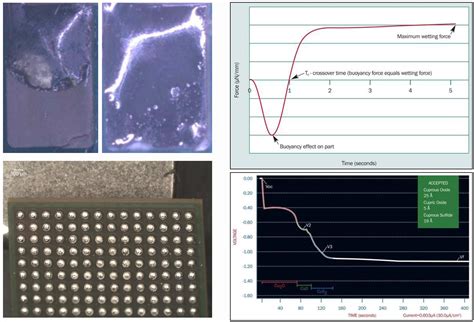
The wetting balance test, also known as the solder meniscus test, is a quantitative method for evaluating the solderability of component leads or PCB pads. In this test, a sample is immersed in a molten solder bath, and the wetting force is measured as a function of time. The test provides information on the speed and extent of solder wetting, as well as the maximum wetting force achieved.
Wetting Balance Test Parameters
| Parameter | Description |
|---|---|
| Immersion depth | The depth to which the sample is immersed in the solder bath (typically 1-2mm) |
| Immersion time | The duration for which the sample is immersed in the solder bath (typically 3-5 seconds) |
| Solder temperature | The temperature of the molten solder bath (typically 235-245°C for tin-lead solder) |
| Wetting force | The force exerted by the molten solder on the sample due to surface tension |
Dip and Look Test
The dip and look test is a qualitative method for assessing the solderability of component leads or PCB pads. In this test, the sample is dipped into a molten solder bath for a specified time and then withdrawn. The soldered surface is visually inspected for the appearance of the solder coating, the presence of dewetting, and the extent of solder coverage.
Dip and Look Test Criteria
| Criteria | Description |
|---|---|
| Solder coverage | The percentage of the surface area covered by the solder coating |
| Solder appearance | The smoothness, brightness, and uniformity of the solder coating |
| Dewetting | The presence of areas where the solder has pulled away from the surface |
| Non-wetting | The presence of areas where the solder has not adhered to the surface |
Solderability Edge Dip Test
The solderability edge dip test is a method for evaluating the solderability of PCB edges and plated through-holes. In this test, the edge of the PCB is dipped into a molten solder bath at a 45-degree angle for a specified time. The soldered edge is then visually inspected for the appearance of the solder coating, the presence of dewetting, and the extent of solder coverage.
Solderability Edge Dip Test Parameters
| Parameter | Description |
|---|---|
| Immersion angle | The angle at which the PCB edge is dipped into the solder bath (typically 45 degrees) |
| Immersion time | The duration for which the PCB edge is immersed in the solder bath (typically 5-10 seconds) |
| Solder temperature | The temperature of the molten solder bath (typically 235-245°C for tin-lead solder) |

Factors Affecting Solderability
Several factors can influence the solderability of components and PCBs. Understanding these factors is essential for maintaining good solderability and preventing soldering defects.
Surface Finish
The surface finish of components and PCBs plays a crucial role in solderability. Common surface finishes include:
- Hot Air Solder Leveling (HASL)
- Electroless Nickel Immersion Gold (ENIG)
- Immersion Silver (ImAg)
- Immersion Tin (ImSn)
- Organic Solderability Preservative (OSP)
Each surface finish has its own characteristics and solderability performance. For example, ENIG provides excellent solderability and shelf life, while OSP is cost-effective but has a limited shelf life.
Storage Conditions
Proper storage conditions are essential for maintaining the solderability of components and PCBs. Factors to consider include:
- Temperature: Components and PCBs should be stored in a cool, dry environment to prevent oxidation and degradation of the surface finish.
- Humidity: High humidity can lead to the formation of corrosion and tarnishing on the surface, reducing solderability.
- Packaging: Components should be stored in moisture-barrier bags with desiccants to prevent moisture ingress and oxidation.
- Shelf Life: The solderability of components and PCBs can degrade over time, so it is important to use them within their specified shelf life.
Contamination
Contamination on the surface of components or PCBs can significantly impact solderability. Common contaminants include:
- Oils and greases from handling
- Flux residues from previous soldering processes
- Dust and debris from the environment
- Oxidation and tarnishing of the surface finish
Proper cleaning and handling procedures should be implemented to minimize contamination and maintain good solderability.

Solderability Testing Standards
Several international standards provide guidelines and requirements for solderability testing. These standards ensure consistency and repeatability in solderability testing methods and help manufacturers meet quality and reliability requirements. Some of the key solderability testing standards include:
- IPC J-STD-002: Solderability Tests for Component Leads, Terminations, Lugs, Terminals, and Wires
- IPC J-STD-003: Solderability Tests for Printed Boards
- IEC 60068-2-20: Environmental Testing – Part 2-20: Tests – Test T: Test methods for solderability and resistance to soldering heat of devices with leads
- MIL-STD-202: Test Method Standard – Electronic and Electrical Component Parts
These standards provide detailed specifications for test methods, sample preparation, test conditions, and acceptance criteria for solderability testing.
Interpreting Solderability Test Results
Interpreting the results of solderability tests is crucial for making informed decisions about component and PCB Quality and soldering process optimization. Some key aspects to consider when interpreting solderability test results include:
Wetting Force
In the wetting balance test, the maximum wetting force achieved indicates the degree of solderability. A higher wetting force generally indicates better solderability, as it demonstrates the ability of the molten solder to wet and adhere to the surface. However, it is important to compare the results against the specific requirements for the application and the acceptable range specified in the relevant standards.
Solder Coverage and Appearance
In the dip and look test and solderability edge dip test, the extent of solder coverage and the appearance of the solder coating provide qualitative information about solderability. Good solderability is characterized by uniform solder coverage, a smooth and shiny appearance, and the absence of dewetting or non-wetting areas. Any irregularities or defects in the solder coating may indicate poor solderability and require further investigation.
Statistical Analysis
When conducting solderability tests on a large number of samples, statistical analysis can provide valuable insights into the overall solderability performance. By calculating metrics such as the mean, standard deviation, and process capability indices (Cp and Cpk), manufacturers can assess the consistency and reliability of their soldering processes and identify areas for improvement.
Frequently Asked Questions (FAQ)
-
What is the purpose of solderability testing?
The purpose of solderability testing is to evaluate the ability of electronic components and PCBs to be soldered effectively. It assesses the wettability and adhesion properties of the surfaces to be soldered, ensuring reliable electrical connections and mechanical strength. -
What are the most common solderability tests?
The most common solderability tests include the wetting balance test, dip and look test, and solderability edge dip test. Each test has its own specific methodology and provides different types of information about solderability. -
How does surface finish affect solderability?
The surface finish of components and PCBs plays a crucial role in solderability. Different surface finishes, such as HASL, ENIG, ImAg, ImSn, and OSP, have their own characteristics and solderability performance. The choice of surface finish depends on factors such as cost, shelf life, and the specific requirements of the application. -
How can solderability issues be prevented?
Solderability issues can be prevented by implementing proper storage conditions, handling procedures, and cleaning processes. Components and PCBs should be stored in a cool, dry environment, with appropriate packaging to prevent moisture ingress and oxidation. Contamination should be minimized through careful handling and regular cleaning of the surfaces to be soldered. -
What are the benefits of conducting solderability testing?
Conducting solderability testing offers several benefits, including quality assurance, process optimization, cost reduction, and regulatory compliance. By identifying solderability issues early, manufacturers can avoid using substandard components, reduce the occurrence of soldering defects, improve production efficiency, and meet the required quality and reliability standards for their products.
Conclusion
Solderability testing is an essential process in the electronics manufacturing industry, ensuring the reliability and quality of soldered connections. By understanding the different types of solderability tests, the factors affecting solderability, and the relevant testing standards, manufacturers can effectively assess and optimize their soldering processes. Regular solderability testing, combined with proper storage, handling, and cleaning procedures, can help prevent soldering defects, reduce costs, and improve the overall performance of electronic assemblies.


Leave a Reply