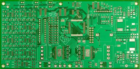
What is a Single-Layer PCB?
A single-layer PCB, also known as a single-sided PCB, is a printed circuit board that has conductive traces and components on only one side of the board. The other side of the board is typically left bare or coated with a solder mask for protection. Single-layer PCBs are the simplest and most cost-effective type of PCB, making them a popular choice for simple electronic projects and low-volume production runs.
Advantages of Single-Layer PCBs
- Low cost: Single-layer PCBs are the most affordable type of PCB due to their simple design and manufacturing process.
- Quick turnaround: The manufacturing process for single-layer PCBs is relatively fast, allowing for shorter lead times and faster project completion.
- Easy to design: Designing a single-layer PCB is simpler compared to multi-layer PCBs, as there are fewer design constraints and considerations.
- Suitable for low-complexity circuits: Single-layer PCBs are ideal for simple electronic projects that do not require complex routing or high component density.
Disadvantages of Single-Layer PCBs
- Limited routing options: With only one layer available for routing, single-layer PCBs may require jumper wires or creative routing solutions for more complex circuits.
- Lower component density: Single-layer PCBs have limited space for components, which can restrict the complexity and functionality of the circuit.
- Reduced signal integrity: The lack of a ground plane and the presence of longer traces can lead to increased electromagnetic interference (EMI) and reduced signal integrity compared to multi-layer PCBs.
- Not suitable for high-speed designs: Single-layer PCBs are not recommended for high-speed or high-frequency designs due to their limited ability to control impedance and minimize crosstalk.
Manufacturing Process of Single-Layer PCBs
Step 1: PCB Design
The first step in manufacturing a single-layer PCB is to create the PCB design using CAD software. The designer must ensure that the design adheres to the limitations of single-layer PCBs, such as avoiding overlapping traces and minimizing the use of jumper wires.
Step 2: PCB Fabrication
Once the design is finalized, the PCB fabrication process begins. The main steps involved in fabricating a single-layer PCB are:
- Substrate preparation: A copper-clad laminate, typically made of FR-4 material, is cut to the desired size and shape.
- Drilling: Holes are drilled into the substrate for component leads and vias, if required.
- Copper etching: The unwanted copper is removed from the substrate using a chemical etching process, leaving behind the desired conductive traces.
- Solder mask application: A protective solder mask is applied to the PCB surface, exposing only the areas where components will be soldered.
- Silkscreen printing: Text, symbols, and logos are printed onto the PCB surface using silkscreen printing for easy identification and assembly.
Step 3: PCB Assembly
After the PCB is fabricated, the components are placed and soldered onto the board. For single-layer PCBs, this process is typically done using through-hole technology (THT), where component leads are inserted through the drilled holes and soldered on the opposite side of the board.
Step 4: Testing and Inspection
The assembled PCB undergoes thorough testing and inspection to ensure proper functionality and quality. This may include visual inspection, automated optical inspection (AOI), and electrical testing.

Design Considerations for Single-Layer PCBs
When designing a single-layer PCB, there are several key considerations to keep in mind:
- Trace width and spacing: Ensure that the trace width and spacing are sufficient to handle the required current and voltage while minimizing the risk of short circuits and signal interference.
- Component placement: Optimize component placement to minimize trace lengths and crossing, and to facilitate efficient assembly and soldering.
- Jumper wires: If necessary, use jumper wires to create connections that cannot be routed directly on the single layer. However, minimize the use of jumper wires as they can increase assembly time and reduce reliability.
- Routing techniques: Employ routing techniques such as 45-degree angles and curved traces to improve signal integrity and minimize electromagnetic interference.
- Solder mask and silkscreen: Use solder mask and silkscreen to protect the PCB surface and provide clear labeling for components and orientation.

Applications of Single-Layer PCBs
Single-layer PCBs are widely used in various applications, particularly in simple electronic projects and low-volume production runs. Some common applications include:
- Consumer electronics: Toys, remote controls, calculators, and simple appliances.
- Prototyping and hobbyist projects: Arduino shields, breadboard adapters, and DIY electronics projects.
- Low-power devices: LED lighting, simple sensors, and battery-powered devices.
- Educational purposes: Teaching basic electronics and PCB design principles to students and beginners.

Frequently Asked Questions (FAQ)
1. What is the difference between a single-layer PCB and a double-layer PCB?
A single-layer PCB has conductive traces and components on only one side of the board, while a double-layer PCB has conductive traces and components on both sides of the board. Double-layer PCBs offer more routing options and higher component density compared to single-layer PCBs.
2. Can single-layer PCBs be used for high-current applications?
Single-layer PCBs can be used for high-current applications, but the trace width and copper thickness must be carefully designed to handle the required current without excessive heating or voltage drop. In some cases, it may be more appropriate to use a double-layer or multi-layer PCB for high-current applications.
3. How can I optimize the design of a single-layer PCB?
To optimize the design of a single-layer PCB, consider the following tips:
- Minimize trace lengths and crossing
- Use appropriate trace width and spacing for the required current and voltage
- Employ routing techniques such as 45-degree angles and curved traces
- Optimize component placement for efficient assembly and soldering
- Use jumper wires sparingly and only when necessary
4. What are the typical materials used for single-layer PCBs?
The most common material used for single-layer PCBs is FR-4, a glass-reinforced epoxy laminate. Other materials, such as aluminum, copper, or flexible substrates, can also be used depending on the specific application requirements.
5. Are single-layer PCBs suitable for high-frequency designs?
Single-layer PCBs are generally not recommended for high-frequency designs due to their limited ability to control impedance and minimize crosstalk. For high-frequency applications, multi-layer PCBs with dedicated ground and power planes are typically used to ensure better signal integrity and electromagnetic compatibility.
Conclusion
Single-layer PCBs are a cost-effective and efficient solution for simple electronic projects and low-volume production runs. Despite their limitations in terms of routing options and component density, single-layer PCBs remain a popular choice for many applications due to their low cost, quick turnaround, and ease of design.
When designing a single-layer PCB, it is essential to consider factors such as trace width and spacing, component placement, routing techniques, and the use of jumper wires. By carefully optimizing the design and following best practices, engineers and hobbyists can create reliable and functional single-layer PCBs that meet their project requirements.
As the demand for simple and affordable electronic solutions continues to grow, single-layer PCBs will likely remain an important part of the electronics industry, serving as a gateway for beginners and a reliable option for low-complexity projects.


Leave a Reply