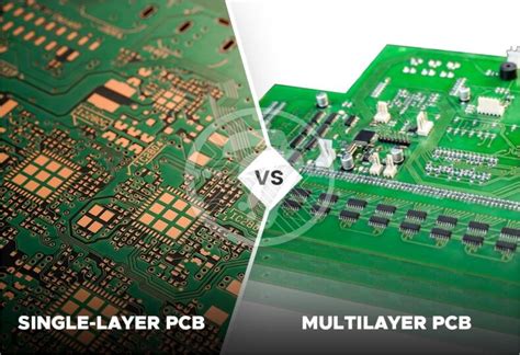
Introduction to Single-Layer PCBs
A single-layer printed circuit board (PCB) is the simplest and most cost-effective type of PCB, consisting of a single conductive layer of copper traces and pads on an insulating substrate material. Single-layer PCBs are ideal for low-density electronic designs with a limited number of components and interconnections. They are widely used in various applications, including consumer electronics, hobbyist projects, and prototyping.
Advantages of Single-Layer PCBs
Single-layer PCBs offer several advantages over more complex multi-layer boards:
- Cost-effectiveness: Single-layer PCBs are the most affordable option due to their simple construction and minimal material requirements.
- Faster production: The manufacturing process for single-layer PCBs is relatively quick, as there are fewer steps involved compared to multi-layer boards.
- Easier design: Designing a single-layer PCB is less complex than multi-layer boards, making it suitable for beginners and hobbyists.
- Simplified troubleshooting: With all components and traces on one side, identifying and resolving issues on a single-layer PCB is more straightforward.
Limitations of Single-Layer PCBs
While single-layer PCBs are suitable for many applications, they have some limitations:
- Limited complexity: Single-layer PCBs are not suitable for high-density designs with a large number of components and interconnections.
- Reduced signal integrity: As the trace density increases, single-layer PCBs are more susceptible to electromagnetic interference and crosstalk.
- Limited power handling: Single-layer PCBs may not be able to handle high-current or high-voltage applications due to the limited copper thickness and trace width.
Designing Single-Layer PCBs
PCB Design Software
To create a single-layer PCB, you will need to use PCB design software. There are various options available, ranging from free open-source tools to professional-grade software. Some popular PCB design software include:
| Software | License | Ease of Use | Features |
|---|---|---|---|
| KiCad | Open-source | Beginner-friendly | Schematic capture, PCB layout, 3D viewer |
| Eagle | Commercial (free version available) | Intermediate | Schematic capture, PCB layout, extensive component libraries |
| Altium Designer | Commercial | Advanced | Schematic capture, PCB layout, simulation, high-end features |
Schematic Design
The first step in designing a single-layer PCB is to create a schematic diagram of your circuit. A schematic represents the electrical connections between components using symbols and lines. When designing your schematic, consider the following:
- Component selection: Choose components that are suitable for your application and available in packages that can be easily soldered to a single-layer PCB.
- Power supply: Ensure that your power supply is adequate for your circuit’s requirements and that you have included appropriate voltage regulation and filtering.
- Grounding: Proper grounding is essential for circuit stability and noise reduction. Create a solid ground plane and connect all ground points to it.
PCB Layout
Once your schematic is complete, you can proceed to the PCB layout stage. During this process, you will arrange components and route traces on the single-layer board. Keep these tips in mind:
- Component placement: Place components in a logical order, minimizing the distance between connected components to reduce trace lengths and improve signal integrity.
- Trace routing: Route traces efficiently, avoiding sharp angles and minimizing crossovers. Ensure that traces are wide enough to handle the required current and that there is sufficient clearance between traces to prevent short circuits.
- Copper pour: Create a copper pour (also known as a ground plane) to provide a low-impedance return path for signals and improve EMI performance.
- Silkscreen: Add silkscreen labels to identify components, connectors, and other important features on the PCB.

Manufacturing Single-Layer PCBs
PCB Fabrication Process
The manufacturing process for single-layer PCBs involves several steps:
- Substrate preparation: The insulating substrate material (usually FR-4) is cut to the desired size and shape.
- Copper cladding: A thin layer of copper foil is laminated onto the substrate using heat and pressure.
- Drilling: Holes are drilled through the board for through-hole components and vias.
- Photoresist application: A light-sensitive photoresist is applied to the copper surface.
- Exposure and development: The photoresist is exposed to UV light through a photomask, which hardens the exposed areas. The unexposed areas are then removed using a developer solution.
- Etching: The exposed copper is etched away using a chemical solution, leaving only the desired traces and pads.
- Solder mask application: A protective solder mask is applied to the board, covering the copper traces but leaving the pads exposed.
- Silkscreen printing: The silkscreen labels are printed onto the solder mask using ink.
- Surface finish: A surface finish (such as HASL, ENIG, or OSP) is applied to the exposed pads to prevent oxidation and improve solderability.
PCB Material Selection
The most common substrate material for single-layer PCBs is FR-4, a glass-reinforced epoxy laminate. FR-4 offers good mechanical strength, electrical insulation, and thermal stability. Other substrate materials include:
| Material | Properties | Applications |
|---|---|---|
| CEM-1 | Lower cost and performance than FR-4 | Consumer electronics, low-end applications |
| Polyimide | High temperature resistance, flexibility | Aerospace, military, flexible circuits |
| Aluminum | Excellent thermal conductivity | High-power LED lighting, heatsinks |
For the copper layer, the standard thickness is 1 oz/ft² (35 µm), although thicker options (2 oz/ft² or 70 µm) are available for high-current applications.
PCB Assembly
After the PCB fabrication process, the board is ready for assembly. Single-layer PCBs can be assembled using either through-hole or surface-mount components.
- Through-hole assembly: Components with leads are inserted into the drilled holes and soldered to the pads on the opposite side of the board.
- Surface-mount assembly: Components are placed directly onto the pads on the same side of the board and soldered using a reflow oven or hand soldering.
When assembling your single-layer PCB, consider the following:
- Soldering techniques: Use the appropriate soldering iron, tip size, and temperature for your components and board. Apply solder sparingly and ensure that joints are clean and shiny.
- Electrostatic discharge (ESD) protection: Use an ESD-safe workspace and tools to prevent damage to sensitive components during assembly.
- Inspection: Visually inspect your assembled board for soldering defects, short circuits, and misaligned components.

Testing and Troubleshooting Single-Layer PCBs
Continuity Testing
After assembly, perform a continuity test to ensure that all connections are correctly made and that there are no short circuits. Use a multimeter to:
- Check for shorts: Test for continuity between ground and power points, as well as between adjacent traces. A low resistance reading indicates a short circuit.
- Verify connections: Check for continuity between connected points on the board, such as component pins and pads. A high resistance reading or open circuit indicates a poor connection.
Power-on Testing
Once you have verified the continuity of your board, apply power and test its functionality. Use an oscilloscope or logic analyzer to:
- Check power supply voltages: Ensure that the power supply voltages are within the expected ranges and free from excessive noise or ripple.
- Verify signal integrity: Observe the waveforms at critical points in your circuit to ensure that signals are clean and free from distortion, ringing, or crosstalk.
Troubleshooting Techniques
If your single-layer PCB is not functioning as expected, use these troubleshooting techniques:
- Visual inspection: Carefully examine the board for visible defects, such as solder bridges, cold solder joints, or damaged components.
- Isolate the problem: Divide the circuit into sections and test each section independently to isolate the source of the issue.
- Check components: Test individual components for proper functionality using a multimeter or component tester.
- Review the schematic and layout: Double-check your schematic and PCB layout for design errors or inconsistencies.

Frequently Asked Questions (FAQ)
1. What is the minimum trace width for a single-layer PCB?
The minimum trace width depends on the PCB manufacturer’s capabilities and the required current carrying capacity. A common minimum trace width for a single-layer PCB is 0.006 inches (0.15 mm), but some manufacturers may offer finer traces down to 0.003 inches (0.075 mm).
2. Can single-layer PCBs be used for high-frequency applications?
Single-layer PCBs can be used for high-frequency applications up to a certain point. However, as the frequency increases, the risk of signal integrity issues, such as crosstalk and electromagnetic interference, also increases. For high-frequency applications, multi-layer PCBs with proper grounding and shielding are generally recommended.
3. What is the maximum number of components that can be placed on a single-layer PCB?
The maximum number of components on a single-layer PCB depends on the board size, component sizes, and layout complexity. As a general rule, single-layer PCBs are suitable for designs with up to 50-100 components. For higher component counts, a multi-layer PCB may be more appropriate.
4. Can single-layer PCBs be used for surface-mount components?
Yes, single-layer PCBs can be used with surface-mount components. However, the layout and soldering process may be more challenging compared to through-hole components, especially for fine-pitch components or high-density layouts.
5. Are there any special considerations when designing single-layer PCBs for automated assembly?
When designing single-layer PCBs for automated assembly, consider the following:
- Component placement: Ensure that components are spaced far enough apart to allow for the automated pick-and-place machine’s tolerances.
- Solder mask and paste: Use a solder mask to prevent solder bridges and ensure that the solder paste stencil apertures are appropriate for your components.
- Fiducial markers: Include fiducial markers on your board to help the pick-and-place machine align the board and components accurately.
Conclusion
Single-layer PCBs are a simple, cost-effective solution for low-density electronic designs. By understanding the advantages, limitations, and design considerations of single-layer PCBs, you can create functional and reliable circuits for a wide range of applications. When designing and manufacturing your single-layer PCB, pay close attention to component selection, layout, and assembly techniques to ensure optimal performance and reliability.


Leave a Reply