Introduction to Semi Rigid Flex PCBs
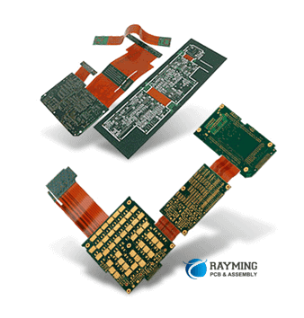
A semi rigid flex PCB is a type of printed circuit board that combines rigid and flexible materials to create a hybrid design. These boards provide the benefits of both rigid boards, like stability and ease of assembly, along with the advantages of flex circuits, including dynamic flexing ability and reduced weight.
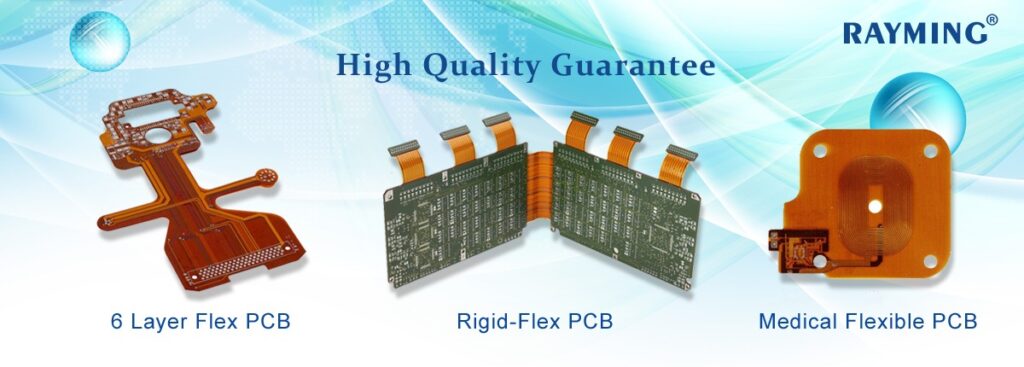
Semi rigid flex PCBs are created by sandwiching flexible dielectric materials between outer layers of rigid laminate. Common rigid materials include FR-4, polyimide, and PTFE composites. The flexible dielectric is often polyimide or other high-temperature thermoplastic films. Rigid sections provide mechanical stability for mounting components, while flexible sections allow dynamic movement and improved reliability through flexing.
Semi rigid flex boards are ideal for applications that require:
- Dynamic flexing and vibration absorption
- Compact, space-saving PCB designs
- Integration of rigid and flexible materials
- Stable component mounting combined with flexible interconnections
They are commonly used in industries like aerospace, defense, telecommunications, medical, and consumer electronics.
Benefits of Using Semi Rigid Flex PCBs
Here are some of the key benefits provided by semi rigid flex PCBs:
Dynamic Flexing Ability
The flexible portions of the PCB can bend and flex repeatedly. This absorbs vibration, shock, and thermal cycling in demanding environments. The rigid sections maintain stability for component mounting.
Lightweight and Compact Design
Thin flexible dielectric materials reduce weight and bulkiness. Semi rigid flex PCBs can fit into tight spaces and enable smaller product enclosures.
Reliability and Durability
The flexible areas accommodate movement and flexing to improve reliability and durability under dynamic operating conditions. This reduces failures from cracked solder joints and plated through holes (PTHs).
Efficient Routing and Layer Stackup
Flexible sections enable more trace routing layers in a confined space. This facilitates complex layouts and minimizes the need for jumper wires.
Reduced Assembly Costs
Integrating flex and rigid materials into one PCB can eliminate the need for connectors between separate boards. This reduces overall assembly time and costs.
Design Flexibility
Semi rigid flex PCBs enable creative solutions by combining the best aspects of rigid and flex PCBs into a single design. The PCB layout can be optimized based on performance requirements.
Typical Design and Construction
Semi rigid flex PCBs can be constructed using different layer counts, stackups, and layouts depending on the design needs. Here are some typical design considerations:
Layer Stackup
A basic 4-layer stackup consists of:
- Rigid laminate outer layers
- Flexible dielectric inner layers
- Copper traces between the dielectric layers
Additional layers can be added to allow more trace routing or shielding ground planes. Common layer counts range from 4 to 12 or more.
Rigid vs Flex Areas
The PCB layout defines the placement of rigid and flexible zones. Component dense regions are typically rigid. Interconnect areas benefit from flexible construction. Rigid sections may comprise 20-80% of the total area.
Component Mounting
Components are typically mounted only in rigid zones which provide mechanical stability. Flexible areas may contain only PTHs and traces. However, some designs allow small, lightweight components in flex zones.
Transitions Between Rigid and Flex
The junction between rigid and flexible materials is carefully managed to avoid mechanical stress. Creepage distance rules must also be observed.
Shielding Considerations
Sensitive traces may need shielding in flex zones. This can be achieved by adding grounded copper layers or shields around the flex area.
Stiffener Plates
Metal stiffener plates are often added to strengthen the PCB at critical rigid-flex junctions or high-stress points. Stiffeners prevent flex cracks.
Material Selection Considerations
Several materials factors must be evaluated when designing a semi rigid flex PCB:
Rigid Laminate Materials
FR-4, polyimide, PTFE composites, FR-2, and CEM-1 are commonly used. Material choice depends on operating temperature range, stability, and dielectric requirements.
Flexible Dielectric Films
Polyimide films like Kapton or Upilex provide excellent flexibility and high temperature resistance. Other options include PEEK or polyethylene naphthalate (PEN). Thickness is typically 2 to 5 mils.
Copper Foil Thickness
Thicker copper (2 oz/ft2 or greater) is used in rigid sections while thinner foils (1/2 to 1 oz/ft2 ) are used in flex areas. This balances conductivity and flexibility.
Coverlay/Masking Materials
Polyimide, acrylic, or epoxy coverlay materials are applied to both sides to protect traces. Photoimageable coverlays allow selective openings for soldering.
Adhesives
Acrylic or epoxy adhesives bind the material layers into a unified board. They must withstand flexing stresses and thermal expansion differences between layers.
Manufacturing Processes
Specialized fabrication processes are required to manufacture semi rigid flex PCBs:
Imaging and Etching
Photolithographic imaging and etching techniques pattern the copper traces on each layer. Additive plating can also be used to plate up trace designs.
Layer Alignment and Registration
Layers must be precisely aligned to ensure reliable interlayer connections through PTHs and vias during the lamination process. Misalignments create reliability risks.
Sheet Cutting
The rigid and flex materials are supplied in larger sheets and must be cut to the proper outline after imaging the traces. This can be done by lasers, waterjets, or mechanical tools.
Lamination Cycle
The material layers are bonded together in a high heat and pressure lamination press. The parameters must be optimized to ensure strong, reliable bonds between both rigid and flex layers.
Via Formation
PTHs electrically connect layers and are drilled through the rigid sections. Microvias in the flex layers can be laser drilled or photoformed.
Surface Finishes
Immersion plating with nickel/gold deposits protects traces from oxidation and provides solderability. Selective gold plating is also used.
Final Shaping and Singulation
The panels go through final mechanical shaping steps. Depaneling separates individual PCBs from the larger panel format.
Key Design Guidelines
Following are some key guidelines to ensure reliable, manufacturable semi rigid flex PCBs:
- Minimize rigid-to-flex transition areas
- Use gradual curves instead of sharp bends
- Avoid 180° flex folds where possible
- Analyze dynamic and static mechanical strains
- Include stiffeners at transitions as needed
- Account for thermal expansion differences
- Follow minimum trace/space rules in flex zones
- Use tear-drop vias at rigid-flex junctions
- Allow generous keep-out zones around edges
- Review all guidelines with your PCB manufacturer
Applications of Semi Rigid Flex PCBs
Here are some examples of products that benefit from using semi rigid flex PCB designs:
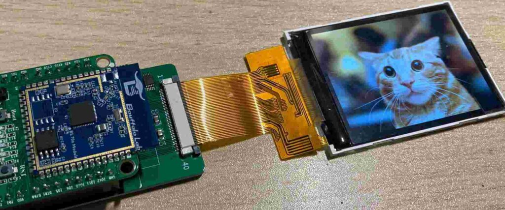
Wearable Electronics
Semi rigid flex PCBs accommodate the dynamic bending and motion involved in wearable devices, while providing stable platforms for mounting components.
Medical Electronics
Combining rigid and flexible materials allows medical devices to withstand repeated flexing in a compact form factor and meet stringent biocompatibility requirements.
Robotics and Automation
The flexing and vibration resistance of these boards supports reliable performance in moving robotic mechanisms and automated machinery.
Defense Electronics
Mission-critical defense and aerospace applications rely on the durability of semi rigid boards under extreme temperatures and dynamic environments.
Consumer Electronics
Portable consumer products like laptops, mobile phones, and tablets must survive everyday shock and vibration. Semi rigid flex PCBs help enable durable, lightweight designs.
Conclusion
Semi rigid flex PCBs provide the ideal combination of mechanical stability, dynamic flex capability, and design flexibility. By integrating the right materials using specialized fabrication processes, semi rigid boards can survive the most demanding operating conditions while supporting cutting-edge circuit designs. As electronics applications continue trending toward lightweight and high-reliability designs, these hybrid PCBs will become increasingly essential across a broad range of industries.
Frequently Asked Questions
What are some typical applications for semi rigid flex PCBs?
Some major applications are aerospace systems, military electronics, mobile devices, automotive electronics, medical instruments, robotics, and any products needing vibration resistance and tight interconnects between multiple PCBs.
What are some key considerations when selecting rigid vs. flex sections?
Component densities, required stiffness, anticipated mechanical strains, and the need for dynamic flexing vs. stability. High-density component areas should use rigid materials while lower-density interconnect zones can be flexible.
How many layers are typical for semi rigid flex designs?
While 4-6 layers are common, some complex designs may use 8 or more layers. Rigid sections often have more layers than flex zones. High layer counts provide more routing space but increase fabrication complexity.
What are some methods used to validate the reliability of semi rigid flex PCBs?
Environmental stress testing including dynamic bend cycles, torsion testing, vibration, mechanical shock, thermal cycling, and simulated lifetime testing are used to validate robustness. Finite element analysis models strains.
How are components assembled onto semi rigid flex PCBs?
Soldering is used to attach components in rigid areas. Flexible regions generally only contain PTHs and traces. Glue can attach light components in flex areas in some cases. Careful design is needed at rigid-flex junctions.
Conclusion
Semi rigid flex PCBs offer the ideal combination of stability, dynamic flexing ability, and design optimization. When fabricated using robust materials and processes, they can survive the harshest operating environments. With emerging applications demanding lightweight, reliable interconnections, these hybrid boards provide an enabling technology across many industries from consumer electronics to mission-critical systems.


Leave a Reply