Rigid printed circuit boards (PCBs) are the backbone of modern electronics. From computers and smartphones to industrial controls and medical devices, rigid PCBs provide the foundation for mounting and interconnecting electronic components. This comprehensive guide covers everything you need to know about rigid PCB materials, design, manufacturing, assembly, and testing.
What is a Rigid PCB?
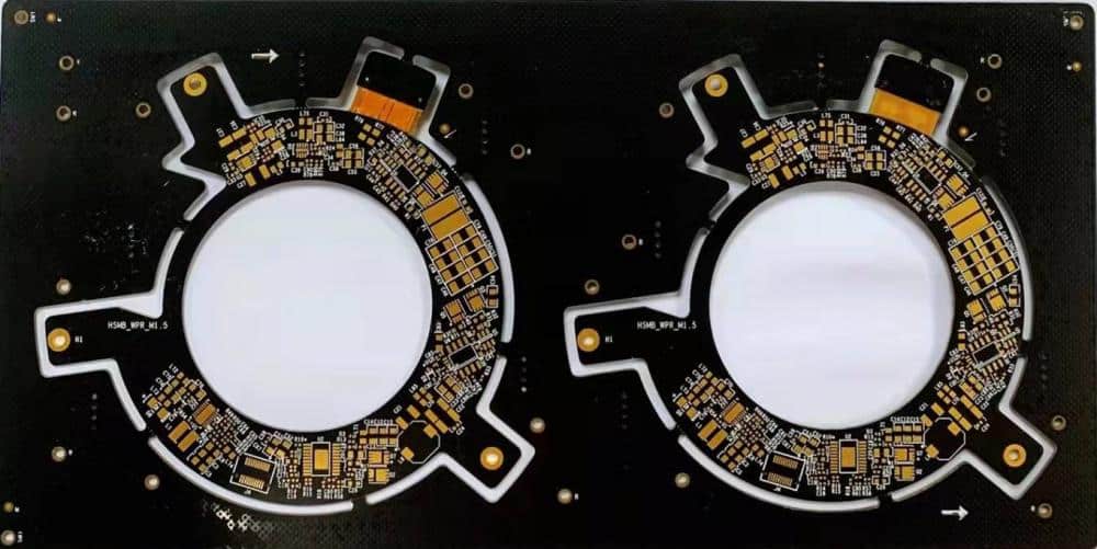
A rigid PCB is a flat, non-flexible circuit board made from rigid insulating substrates like FR-4 or polyimide. The board itself is inflexible and does not bend or flex during use. Rigid PCBs provide mechanical support for mounted components and serve as the electrical interconnection platform between components.
The rigid laminate material that makes up the board provides electrical isolation between conductive traces and acts as a heat sink to dissipate component-generated heat. Conductive traces, pads, and other features are etched from copper foil bonded to the substrate. Plated through holes provide electrical interconnection between layers in multilayer boards.
Rigid PCB Materials
The material used for the insulating substrate is a key determinant of the performance and cost of a rigid PCB. The most common materials used are:
FR-4
FR-4 glass epoxy is the most popular and cost-effective rigid PCB material. The FR-4 substrate consists of woven fiberglass cloth bonded with flame-retardant epoxy resin. FR-4 offers good mechanical strength, dimensional stability, and electrical performance at relatively low cost. However, it has limited thermal conductivity and heat resistance compared to higher-performance substrates.
CEM-1
Cellulose paper reinforced epoxy laminate offers better thermal performance over FR-4 due to its higher glass transition temperature. It has lower moisture absorption and improved dimensional stability over FR-4. CEM-1 is more expensive than FR-4 but cheaper than high-end materials.
Polyimide
Polyimide laminates like Arlon 85N and DuPont Pyralux offer very high heat resistance, thermal conductivity, and dimensional stability. However, polyimide PCBs are significantly more expensive than FR-4 or CEM-1. Polyimide is typically used only when very high temperatures or performance is required.
PTFE
Polytetrafluoroethylene (PTFE) based substrates like Rogers RO4000 series offer excellent electrical performance. PTFE has extremely low dielectric loss, low moisture absorption, and stability across a wide temperature range. PTFE boards are expensive but ideal for high-frequency analog and radio frequency (RF) applications.
| Material | Dielectric Constant | Loss Tangent | Tg | Thermal Conductivity |
|---|---|---|---|---|
| FR-4 | 4.5 | 0.02 | 130°C | 0.25 W/mK |
| CEM-1 | 4.5 | 0.02 | 170°C | 0.42 W/mK |
| Polyimide | 3.4 | 0.003 | 340°C | 0.46 W/mK |
| PTFE | 2.1 | 0.0007 | 270°C | 0.71 W/mK |
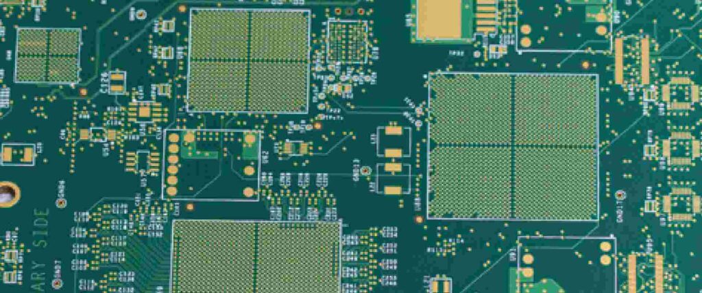
Rigid PCB Design Considerations
Careful design is critical for getting the most performance and reliability out of a rigid PCB. Some key design considerations include:
- Board Layout: Optimize layout for manufacturability, assembly, heat dissipation, and electrical performance. Ensure adequate clearance between traces and components.
- Stackup: Choose layer count, dielectric materials, and trace dimensions appropriately for required current capacity, impedance control, and noise reduction.
- Routing: Use minimum trace widths and clearances for desired current capacity. Use 45° miters and teardrops on traces.
- Planes: Use continuous reference planes for controlled impedance traces. Solid planes also act as heat sinks. Split planes where needed for isolation.
- Vias: Minimize via stubs. Use backdrilling for high-speed signals. Include thermal reliefs where vias connect to large copper regions.
- Materials: Choose dielectric and copper materials appropriate for operating frequency, power levels, and thermal management needs.
- EMI/EMC: Incorporate shielding, filtering, and sound layout practices to meet EMI/EMC requirements.
Thorough design reviews, simulation, and prototyping help verify the design meets all electrical, thermal, and mechanical requirements prior to release for fabrication.
Rigid PCB Fabrication
Rigid PCB fabrication involves many steps to transform the designed layout into a finished circuit board.
Lamination
- Multiple sheets of prepreg dielectric are stacked up with layers of copper foil.
- The stackup is laminated under heat and pressure to form a solid board.
- The lamination process bonds the dielectric layers and copper foils into a single structure.
Drilling
- Small holes are drilled through the board to form vias for layer-to-layer interconnections.
- Highly accurate drilling is critical to ensure vias are properly aligned between layers.
Metallization
- Walls of the drilled holes are plated with copper to form a conductive path between layers.
- Electroless copper followed by electrolytic copper plating metallizes the holes.
Etching
- Photoresist is selectively applied and exposed to define the traced circuit pattern.
- Copper not protected by photoresist is etched away, leaving only the desired traces and features.
Solder Mask and Silkscreen
- Solder mask coats the PCB, leaving only solderable copper features exposed.
- Silkscreen prints visible component designators, logos, and other markings.
- Multiple lamination, drilling, plating, and etching steps are required for multilayer boards with traces on internal layers.
Rigid PCB Assembly
After fabrication, electronic components must be assembled and soldered onto the finished board.
Component Placement
- Components are mounted onto the PCB by automated pick and place machines.
- Reels and sticks feed different component packages to the pick and place heads.
- Optical systems accurately place components onto pads.
Soldering
- Leaded components are inserted through holes in the board.
- Solder paste is screen printed onto pads for surface mount components and leadless packages.
- The assembly is passed through a reflow oven to melt the solder and attach components.
Cleaning and Inspection
- Flux residue is cleaned from the assembled board.
- Automated optical inspection systems check for defects or missing components.
- Electrical testing confirms connectivity and function.
Rigid PCB assembly facilities range from small shops doing prototyping and short runs to high-volume contract manufacturers with fully automated assembly lines.
Rigid PCB Testing
Testing ensures the fabricated and assembled PCBs meet all mechanical, electrical, and performance requirements. Common tests include:
- Netlist Testing: Checks PCB trace connectivity matches circuit netlist.
- In-Circuit Testing: Electrical tests verify components and circuits function properly.
- Flying Probe Testing: Tests connectivity between points without fixtures.
- Automated Optical Inspection: Imaging-based inspection looks for defects and flaws.
- X-Ray Inspection: X-ray imaging looks for potential issues like voids in solder joints.
- Functional Testing: Product-level test of inputs, outputs and functionality.
- Environmental Stress Testing: Evaluates operation under extreme temperature, vibration, etc.
Thorough testing gives confidence in product reliability before PCBs are integrated into electronic devices and systems.
Rigid PCB Applications
The unique benefits of rigid PCBs make them suitable for use across nearly all electronics sectors:
Computers and Servers
Rigid multilayer boards with high interconnect density are widely used in computers, servers, and other digital logic systems. FR-4 is commonly used, with higher performance substrates sometimes used for CPUs and other hot components.
Consumer Electronics
Smartphones, tablets, TVs, and other compact consumer electronics rely on rigid boards. Careful layout and integration of components allow minimizing size while meeting demanding performance requirements.
Automotive Electronics
Automotive control units and infotainment systems use rigid boards proven to withstand vibration, shock, and temperature cycling in vehicle environments. Safety-critical applications require rigorous reliability testing.
Industrial
Industrial electronics for automation, process control, power supplies, instrumentation, and other applications utilize very high reliability rigid PCBs. Rigid-flex boards are often used for interconnections.
High Frequency and RF
Radios, antennas, satellite communications, and radar systems push the limits of rigid PCB electrical performance. High frequency substrates like PTFE and ceramic-filled PTFE are often used.
Medical Electronics
Medical devices use rigid boards proven to function reliably in patient health applications. Biocompatible materials are sometimes used for implanted devices.
Rigid PCB technology provides the backbone for almost every electronic device used today. Continued progress in materials, fabrication processes, and design tools will enable rigid boards to keep pace with the ever-increasing demands of electronics users.
Frequently Asked Questions
What are the key advantages of rigid PCBs compared to flexible PCBs?
Rigid PCBs offer several advantages compared to flexible PCBs:
- Higher layer counts and interconnect density
- Better heat dissipation for high power components
- More robust mechanical structure for support and durability
- Lower and more stable dielectric constant
- Lower cost in high volume
The tradeoff is lack of flexibility – rigid boards cannot bend and flex like flexible circuits. Rigid-flex PCBs combine rigid and flexible substrates for applications requiring both.
How are very dense/complex rigid PCBs manufactured?
High density complex boards like processors and FPGAs use build up process to manufacture the high layer count multilayer boards:
- Core substrate is laminated
- Blind and buried vias are laser drilled and metallized
- Layers are built up sequentially by laminating dielectric and copper
- Microvias create vertical interconnects
- Trace and space is under 5 mils with 2-4 mil typical
The layer count can be over 30 layers to accommodate the I/O density and routing complexity. The boards require very tight process controls.
What are important considerations for rigid PCB layout?
Here are some key rigid PCB layout guidelines:
- Place components for efficient routing, thermal management and manufacturability.
- Leave adequate clearance between traces and pads.
- Use sufficient trace widths for current levels.
- Use appropriate pad shapes and sizes to match components.
- Minimize trace length variations for timing-critical signals.
- Include stitching vias around pads connected to large copper regions.
- Eliminate acuteangles between traces.
- Include text callouts for testpoints and jumpers.
- Partition boards along cut lines to facilitate panelization.
Reviewing layouts, simulation and prototyping are critical to verify satisfactory performance.
How are testpoints designed into a rigid PCB?
Testpoints provide access points to test circuits and signals on a PCB. Recommended practices include:
- Place testpoints so probes can access them. Avoid obstructing components.
- Use dedicated testpads linked to nets rather than oversized component pads.
- Testpads should be greater than 15 mils diameter to allow probe access.
- Link testpads to signals using short traces rather than crowding near components.
- Provide text annotations near testpads identifying names/functions.
- Include ground testpads spaced nearby signals for return paths.
- Testpad size, hole size, and spacing allow using pogo pin fixtures.
What are common defects in rigid PCB fabrication and assembly?
Some typical rigid PCB defects include:
Fabrication
- Shorts or opens due to over/under etching.
- Drill registration errors causing misalignment.
- Plating voids creating poor via conductivity.
- Smearing or lifted traces.
- Holes not properly filled during plating.
Assembly
- Missing or incorrect components placed.
- Insufficient solder.
- Solder bridges between pads.
- Cold solder joints.
- Damaged pads or tracks.
- Flux residue remaining after cleaning.
Careful process controls, inspection, and testing during PCB production help identify and eliminate defects.


Leave a Reply