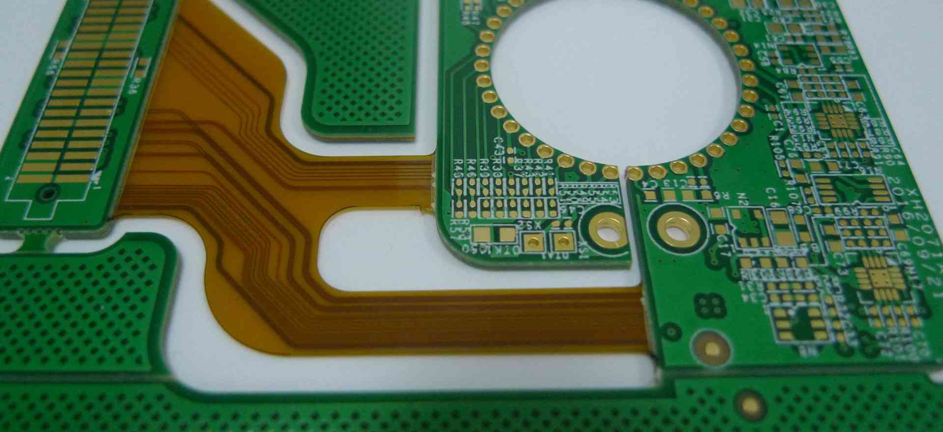
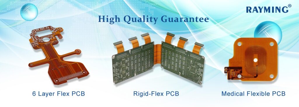
Rigid flex PCBs (printed circuit boards) combine rigid FR-4 boards with flexible circuits bonded together. They provide solutions for complex electronics with space, weight, or wiring constraints. When designing a rigid flex PCB prototype, engineers must consider factors like layer stackup, materials, spacing, and testing.
Designing the Layer Stackup
The layer stackup refers to the sequence of laminated conductive, insulating, and adhesive layers in a PCB. For rigid flex circuits, optimal stackup depends on:
Rigid Sections
- Typical rigid layers use FR-4 substrate with 1 oz copper foil
- Layer count is based on circuit complexity
- High layer counts allow higher component density
Flexible Sections
- Use polyimide films like Kapton® for the flexible substrate
- Copper foils are rolled annealed or electrodeposited
- Keep flexible sections to 2-4 layers for better bending
Bonding Layers
- Adhesive films bond the rigid and flex layers
- Common adhesives are acrylic or epoxy-based
- Keep adhesive thickness under 0.002″ to avoid flexibility loss
Examples
| Section | Layer Stackup |
|---|---|
| Rigid | FR-4 / Cu / FR-4 / Cu / FR-4 |
| Flexible | PI / Cu / PI / Cu / PI |
| Bonding | FR-4 / Adhesive / PI |
Table 1. Sample rigid flex layer stackups
The optimal stackup balances circuit needs, manufacturing, and reliability. Too many layers can make etching and registration difficult. An experienced PCB designer can recommend layer counts and sequences tailored for each design.
Choosing Materials
Material selection greatly impacts rigid flex performance, especially at the bend areas. Important material considerations include:
- Flexible substrate – Polyimide films like Kapton provide the best elasticity and bend life. Other options are PET and PEN films.
- Conductive layers – Copper is standard. Rolled annealed copper resists fractures from flexing. Electrodeposited copper also works. Stainless steel can be used in high-flex applications.
- Bonding adhesive – Look for a flexible adhesive that bonds well to both the rigid and flex substrates during lamination while allowing bending. Common options are acrylic or epoxy-based films.
- Coverlay – Polyimide coverlay protects conductors at the flexing areas. Ideal thickness is around 0.002″. Thicker coverlay restricts bending.
- Solder mask – Liquid photoimageable solder resist masks the rigid board sections. Flexible options are also available.
- Stiffeners – Optional rigid platelets added for strength at connections between rigid and flex sections.
Material selection requires balancing cost, performance, and manufacturability tradeoffs. Work with experienced flex PCB fabricators when selecting materials for an optimal design.
Allowing for Spacing and Bending
Rigid flex PCB layouts require careful conductor spacing and placement for reliability. Guidelines include:
- Trace widths and spacing – Follow the same rules as rigid PCBs. Keep traces large and spaced widely in the rigid sections. Make flex traces narrower with tighter spacing.
- Flexible area keepouts – Avoid placing pads, vias, and through-holes in the bending sections.
- Breakaway sections – Use small unmasked tabs in the flex area to hold boards together during fabrication. These break easily during assembly.
- Bend radius – Maintain at least a 10X substrate thickness bend radius. Lower radius increases stress.
- Stiffeners – Can be added for strength and to set the final bent shape.
- Bonds – Adhere the flex layer fully to the rigid sections for support.
Prototype and Design Verification
Verifying the design is critical before moving to full production. Steps include:
Prototype Reviews
- Thoroughly inspect bare board prototypes for any fabrication issues
- Check for registration errors, insufficient spacing, debris, etc.
- Optically inspect plating quality and subpath registration
- Correct any issues found and order revised prototypes
Test Coupons
- Include test coupons with various trace widths, spacing, plating, etc.
- Test coupons can be used for quality checks during mass production
Functional Testing
- Assemble prototypes and test electrically
- Verify the circuits meet all functional requirements
- Perform “shake and stress” tests, especially on flexing areas
Pilot Production Run
- Run a small pilot production batch (10-50 units)
- Confirm manufacturing process and yields
- Test units thoroughly over time to confirm reliability
- Make any last tweaks to the design prior to full ramp-up
While time consuming, going through rigorous design verification upfront prevents costly failures during mass production.
Frequently Asked Questions
Here are some common FAQs about rigid flex PCB prototype design:
Q: What is the minimum bend radius for a rigid flex PCB?
A: Most flex circuit suppliers recommend maintaining at least a 10X the dielectric thickness bend radius. For a 0.003” polyimide flexible layer, the minimum bend radius would be 0.030”. Tighter bends increase stress and chance of conductor fracturing.
Q: How many layers can a rigid flex PCB support?
A: Rigid sections can support over 20 layers, but flex sections are usually limited to 2-4 layers. High layer counts make registration difficult and decrease flex durability. A well-designed rigid flex circuit will optimize the layer stackup across rigid and flex sections.
Q: Can components be mounted directly on the flex area?
A: It’s recommended to keep the flex area only for traces and coverlay. Mounting stiff components directly on the flex area negatively impacts bending life. Discrete components can be glued or soldered to the rigid sections only.
Q: What are considerations for rigid-flex connectors?
A: Use generous radii at any rigid-flex junction to prevent tearing. Avoid plated through holes crossing the junction. Provide physical support for connections, such as with stiffeners or clamped housings, to prevent separation. Stress test early prototypes.
Q: How long does rigid flex PCB prototype development take?
A: After completing the design, allow 2-3 weeks to fabricate and assemble initial prototypes. Plan for at least 2-3 design iteration cycles to verify the design before release. Prototyping can take 1-3 months depending on complexity. Work closely with your PCB manufacturer during this process.
Conclusion
Rigid flex PCB technology enables innovative electronic designs, but requires careful planning for reliable performance. By considering layer stackup, materials, layout, spacing, and extensive prototyping, engineers can develop successful rigid flex products. Working closely with an experienced flex PCB supplier optimizes the prototyping process. Rigid flex technology will continue expanding as demands for compact and flexible circuits increase.


Leave a Reply