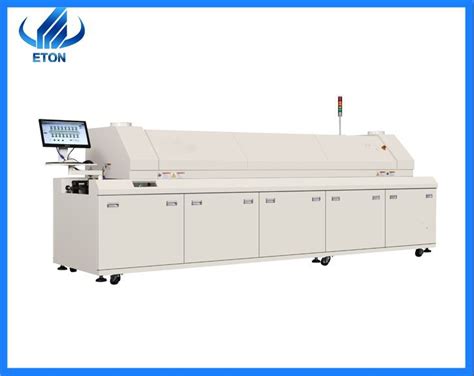
What is Reflow Soldering?
Reflow soldering is a process used to mount electronic components onto printed circuit boards (PCBs) to create permanent electrical connections. It involves applying solder paste to the PCB, placing components, and then heating the entire assembly in a reflow oven to melt the solder and form solder joints.
Reflow soldering has become the standard method for PCB assembly in electronics manufacturing due to its speed, reliability, and ability to produce consistent high-quality solder connections. It can be used for both through-hole and surface mount components.
Key Steps in the Reflow Soldering Process
- Solder Paste Application
- Component Placement
- Reflow
- Cooling
Advantages of Reflow Soldering for PCB Assembly
There are several key advantages of using reflow soldering for PCB assembly compared to other methods like wave soldering or hand soldering:
High Throughput
Reflow soldering is a highly automated process that can assemble PCBs very quickly. Typical reflow ovens have conveyor systems that continuously move PCBs through the oven, allowing high volumes to be processed.
Consistency and Reliability
The reflow process provides very consistent and reliable solder joints across an entire PCB. Parameters like solder paste volume, component placement, and reflow profile can be tightly controlled to ensure repeatable quality.
Handles Fine-Pitch Components
Reflow soldering excels at soldering small surface mount devices with fine lead pitches that would be difficult or impossible to solder by hand. The solder paste and reflow profile can be optimized for these tiny part geometries.
Fewer Defects
With proper process controls in place, reflow soldering results in fewer soldering defects compared to manual assembly methods. Issues like poor wetting, bridging, or insufficient solder fillets are minimized.

Solder Paste
Solder paste is one of the key materials in the reflow soldering process. It consists of tiny solder powder particles suspended in a thick flux medium. The flux removes surface oxides on the metals being soldered and promotes wetting of the liquid solder to the PCB pads and component leads.
Solder Paste Composition
| Material | Typical Proportion |
|---|---|
| Tin/Lead or Lead-Free Solder Alloy Powder | 80-95% |
| Flux Medium | 5-20% |
The most common solder alloys used are tin-lead (SnPb) and lead-free alloys like tin-silver-copper (SAC). Solder powder particle size is categorized by mesh size, with Type 3 and Type 4 being the most common for reflow.
Solder Paste Application Methods
Solder paste is applied to the PCB prior to component placement. The two main methods are:
Stencil Printing
A laser-cut stainless steel stencil with apertures matching the PCB pads is aligned over the board. Solder paste is dispersed over the stencil surface and spread using a squeegee blade, forcing the paste into the apertures and onto the pads.
Dispensing
For lower volumes or large components, solder paste may be dispensed directly onto the PCB pads using an automated needle dispenser. Parameters like dispense time, pressure, and needle size control the amount of paste dispensed.

Pick and Place
Following solder paste application, the components are placed onto the PCB at their respective locations. For surface mount parts, the leads must be aligned with the solder paste prints on the pads.
Modern pick and place machines use computer vision to identify parts and place them automatically at high speed. Some high-end machines can place over 100,000 parts per hour. For prototypes or low volumes, components may be placed by hand.
The accuracy of component placement is critical, as misaligned parts can cause open or shorted solder joints. Typical placement accuracies for surface mount parts are:
| Component Size | Placement Accuracy |
|---|---|
| Chip components, SOT | ±0.05 mm |
| Quad flat packs, fine-pitch BGA | ±0.025 mm |

Reflow Profile
With the components placed, the PCB is run through a reflow oven which heats the board in a controlled manner to melt the solder paste and permanently attach the parts. The heating process is defined by the reflow profile – a graph of temperature versus time.
A proper reflow profile is essential to forming reliable solder joints. It needs to heat the PCB and components enough to fully melt the solder and allow it to wet the surfaces, but not so much that components are damaged.
The key stages in a typical reflow profile are:
-
Preheat – The PCB is slowly heated to about 150°C to evaporate solvents in the paste and activate the flux. This phase usually lasts 60-90 seconds.
-
Soak – Temperature is held steady to allow an even temperature across the entire PCB assembly. Time above 150°C is usually 60-120 seconds.
-
Reflow – The temperature is ramped up quickly to 20-40°C above the solder’s melting point. Time above liquidus is typically 30-90 seconds.
-
Cooling – The PCB is cooled, solidifying the solder joints. Cooling rate should not exceed 4°C/sec to avoid thermal stress.
Ideal reflow profile parameters vary based on the solder paste formulation, PCB design, and component types. The paste manufacturer will provide a recommended profile as a starting point.
Sample Lead-Free Reflow Profile
| Stage | Temp (°C) | Time (sec) |
|---|---|---|
| Preheat | 25 to 150 | 90 |
| Soak | 150 to 200 | 120 |
| Reflow | 200 to 250 | 30 |
| Peak | 250 | 10 |
| Cooling | 250 to 25 | 60 |
Inspection
After the reflow process, solder joint quality should be inspected to identify any defects. Common issues include:
- Insufficent Wetting – The solder did not fully bond to the pad/lead surfaces
- Bridging – Solder shorts between adjacent leads or pads
- Poor Fillets – Solder joint shapes are not properly formed
- Voids – Trapped gasses create holes in the solder joints
Inspection is typically performed both visually and with automated optical inspection (AOI) systems. Visual inspection can catch gross defects but is subject to operator error. AOI compares images of solder joints against an ideal reference to identify defects at higher speed and repeatability.
X-ray inspection may also be used, especially for area array packages like BGAs where the solder joints are not visible from the surface.
Troubleshooting Reflow Soldering Issues
When defects are found, there are several potential root causes to investigate in the reflow process:
Solder Paste
- Paste is old or expired
- Paste storage conditions are improper
- Stencil aperture or dispense needle size is incorrect
- Poor aperture-to-pad alignment in stencil printing
Component Placement
- Component is misaligned or tombstoned
- Lead-to-paste registration is off
- Part is missing or wrong part is placed
Reflow Profile
- Preheat or soak temperature/duration is insufficient
- Peak temperature is too low to fully melt solder
- Time above liquidus is too short
- Ramp rates are too fast, causing thermal shock
Careful process controls and monitoring are essential to minimize reflow soldering defects. Regular cleaning and maintenance of paste printers, pick-and-place machines, and reflow ovens will also help ensure consistent results.
Frequently Asked Questions
What is the difference between reflow and wave soldering?
Reflow soldering is used for surface mount PCB assembly and involves melting solder paste in an oven. Wave soldering immerses the bottom of the PCB in molten solder and is used for through-hole components. Reflow provides more precise control and works with smaller parts.
Can reflow soldering be used for through-hole components?
In general, no. Through-hole reflow requires special paste formulations and component packaging to get solder to wick through the holes. The vast majority of through-hole PCBs are wave soldered.
What type of solder paste should I use?
The main factors in selecting a solder paste are the alloy type (leaded or lead-free), powder particle size, and flux activity level. Consult with your component suppliers and assembly vendor to determine the appropriate grade of solder paste for your application.
How important is the reflow profile?
Creating the right reflow profile is critical to achieving high-quality reflow solder joints. The temperatures and durations of each zone must be carefully tuned to ensure full solder melting and wetting while minimizing thermal stress on components.
What are some common causes of reflow soldering defects?
Common root causes include expired or improperly stored solder paste, inaccurate stencil printing or dispensing, misaligned or missing components, and reflow profiles with insufficient temperatures or times. Careful process control is required to minimize reflow defects.


Leave a Reply