What are QFP and QFN Packages?
Quad Flat Package (QFP)
A Quad Flat Package (QFP) is a surface-mount IC package with leads extending from all four sides of the package. The leads are bent downwards and outwards, forming a “gull-wing” shape. QFP packages are available in various sizes, with the number of leads ranging from 32 to 256 or more. The pitch, or the distance between the leads, can vary from 0.4mm to 1.0mm, depending on the package size and the number of leads.
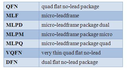
Quad Flat No-lead (QFN)
A Quad Flat No-lead (QFN) package is a surface-mount IC package that does not have any leads extending from the sides. Instead, the electrical connections are made through exposed pads on the bottom of the package. QFN packages are typically smaller than QFP packages, with sizes ranging from 1mm x 1mm to 12mm x 12mm. The pitch of the pads can be as small as 0.4mm, allowing for a high density of connections.
Advantages and Disadvantages of QFP and QFN Packages
Advantages of QFP Packages
- Ease of inspection: The leads on QFP packages are visible and can be easily inspected for soldering defects or damage.
- Compatibility with older equipment: QFP packages have been in use for decades and are compatible with a wide range of manufacturing and testing equipment.
- Better thermal dissipation: The leads on QFP packages act as heat spreaders, allowing for better thermal dissipation compared to QFN packages.
Disadvantages of QFP Packages
- Larger footprint: QFP packages have a larger footprint compared to QFN packages due to the presence of leads, which can be a disadvantage in space-constrained applications.
- Higher inductance: The leads on QFP packages have higher inductance compared to the pads on QFN packages, which can affect high-frequency performance.
- Susceptibility to mechanical damage: The leads on QFP packages are exposed and can be easily damaged during handling or assembly.
Advantages of QFN Packages
- Smaller footprint: QFN packages have a smaller footprint compared to QFP packages, making them suitable for space-constrained applications.
- Lower inductance: The exposed pads on QFN packages have lower inductance compared to the leads on QFP packages, which can improve high-frequency performance.
- Better thermal performance: QFN packages have a large exposed pad on the bottom that can be soldered directly to the PCB, providing a low-resistance thermal path for heat dissipation.
Disadvantages of QFN Packages
- Difficulty in inspection: The lack of visible leads on QFN packages makes it difficult to inspect for soldering defects or damage.
- Compatibility issues: QFN packages may require specialized manufacturing and testing equipment, which can be a disadvantage for some companies.
- Thermal stress: The large exposed pad on QFN packages can cause thermal stress on the PCB due to the difference in thermal expansion coefficients between the package and the board.

Applications of QFP and QFN Packages
QFP and QFN packages are used in a wide range of applications, from consumer electronics to industrial and automotive systems. The choice between QFP and QFN depends on various factors, such as the available space, the required performance, and the manufacturing capabilities.
Applications of QFP Packages
- Microcontrollers and processors: QFP packages are commonly used for housing microcontrollers and processors in embedded systems, such as home appliances, industrial control systems, and automotive electronics.
- Analog and mixed-signal ICs: QFP packages are suitable for analog and mixed-signal ICs, such as operational amplifiers, data converters, and power management ICs, due to their good thermal dissipation and compatibility with older manufacturing equipment.
- Telecommunications and networking: QFP packages are used in telecommunications and networking equipment, such as routers, switches, and modems, where the larger footprint and better thermal dissipation are advantageous.
Applications of QFN Packages
- Wireless communication: QFN packages are widely used in wireless communication devices, such as smartphones, tablets, and IoT devices, due to their small footprint and low inductance, which are essential for high-frequency performance.
- Wearable electronics: The small size and low profile of QFN packages make them suitable for wearable electronics, such as smartwatches, fitness trackers, and medical devices.
- Automotive electronics: QFN packages are increasingly used in automotive electronics, such as advanced driver assistance systems (ADAS), infotainment systems, and engine control units, where the small size and good thermal performance are important.

Comparison Table: QFP vs QFN
| Feature | QFP | QFN |
|---|---|---|
| Leads | Gull-wing leads on all four sides | No leads, exposed pads on the bottom |
| Package Size | Larger, typically 7mm x 7mm to 40mm x 40mm | Smaller, typically 1mm x 1mm to 12mm x 12mm |
| Pitch | 0.4mm to 1.0mm | As small as 0.4mm |
| Footprint | Larger due to the presence of leads | Smaller, suitable for space-constrained applications |
| Thermal Dissipation | Good, leads act as heat spreaders | Better, large exposed pad provides a low-resistance thermal path |
| High-Frequency Performance | Higher inductance due to leads | Lower inductance, better high-frequency performance |
| Inspection | Easy, leads are visible | Difficult, no visible leads |
| Compatibility | Compatible with older equipment | May require specialized equipment |

Frequently Asked Questions (FAQ)
-
Q: Can QFP and QFN packages be used interchangeably?
A: While both QFP and QFN packages serve the same purpose of housing ICs, they have different footprints and require different PCB layouts. Therefore, they cannot be used interchangeably without modifying the PCB design. -
Q: Which package is better for high-frequency applications, QFP or QFN?
A: QFN packages are generally better for high-frequency applications due to their lower inductance and smaller package size. The exposed pads on QFN packages provide a more direct connection to the PCB, reducing the overall inductance of the package. -
Q: How does the thermal performance of QFP and QFN packages compare?
A: QFN packages typically have better thermal performance compared to QFP packages. The large exposed pad on the bottom of QFN packages provides a low-resistance thermal path for heat dissipation, allowing for more efficient cooling of the IC. -
Q: Are QFP packages being phased out in favor of QFN packages?
A: While QFN packages are gaining popularity due to their smaller size and better high-frequency performance, QFP packages are still widely used in many applications. The choice between QFP and QFN depends on the specific requirements of the application, such as available space, thermal dissipation, and compatibility with existing manufacturing equipment. -
Q: Can QFN packages be inspected for soldering defects?
A: Inspecting QFN packages for soldering defects can be challenging due to the lack of visible leads. However, various inspection techniques, such as X-ray imaging, can be used to detect soldering issues in QFN packages.
Conclusion
QFP and QFN packages are both widely used surface-mount packages for integrated circuits, each with its own advantages and disadvantages. QFP packages offer ease of inspection, compatibility with older equipment, and better thermal dissipation, while QFN packages provide a smaller footprint, lower inductance, and better thermal performance.
The choice between QFP and QFN depends on the specific requirements of the application, such as available space, required performance, and manufacturing capabilities. As technology continues to advance, it is likely that both QFP and QFN packages will continue to evolve and find use in a wide range of industries, from consumer electronics to automotive systems and beyond.


Leave a Reply