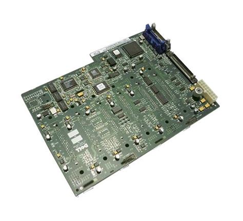
Introduction to PWB
Printed Wiring Boards (PWBs), also known as Printed Circuit Boards (PCBs), are essential components in modern electronics. They provide a platform for mounting and interconnecting electronic components, such as resistors, capacitors, integrated circuits, and connectors. PWBs are used in a wide range of applications, from consumer electronics and telecommunications to aerospace and military systems.
History of PWB
The concept of printed wiring boards dates back to the early 20th century. In 1903, Albert Hanson, a German inventor, filed a patent for a method of creating an electrical connection by bonding metal strips onto an insulating board. However, it wasn’t until the 1920s that the first practical printed circuit was developed by Charles Ducas, an American inventor.
During World War II, the demand for compact and reliable electronic equipment led to further advancements in PWB technology. The U.S. Army Signal Corps collaborated with the National Bureau of Standards to develop a process for printing electrical circuits on insulating boards. This process, known as the “Auto-Sembly” process, revolutionized the electronics industry and laid the foundation for modern PWB manufacturing.
Advantages of PWB
PWBs offer several advantages over traditional point-to-point wiring:
-
Compact size: PWBs allow for the miniaturization of electronic devices by providing a compact and efficient means of interconnecting components.
-
Reliability: The use of printed circuits reduces the risk of wiring errors and improves the overall reliability of electronic systems.
-
Mass production: PWBs can be manufactured in large quantities using automated processes, reducing production costs and time.
-
Consistency: Automated PWB manufacturing ensures consistent quality and reduces the variability associated with manual wiring.
-
Design flexibility: PWBs can be designed to accommodate a wide range of component sizes and configurations, enabling the creation of complex electronic systems.
PWB Manufacturing Process
The manufacturing process for PWBs involves several key steps:
1. Design and Layout
The first step in PWB manufacturing is the design and layout of the circuit. This involves creating a schematic diagram of the electronic circuit and converting it into a physical layout that specifies the location and interconnection of components on the board. Computer-aided design (CAD) software is commonly used for this purpose.
2. Substrate Preparation
The substrate, typically a glass-reinforced epoxy laminate, is cut to the desired size and shape. Copper foil is then laminated onto one or both sides of the substrate using heat and pressure. The copper foil serves as the conductive layer for the printed circuit.
3. Patterning
The desired circuit pattern is transferred onto the copper-clad substrate using a photolithographic process. This involves applying a light-sensitive photoresist layer onto the copper foil and exposing it to UV light through a photomask containing the circuit pattern. The exposed areas of the photoresist are then developed and removed, leaving the desired circuit pattern on the copper foil.
4. Etching
The unwanted copper is removed from the substrate using a chemical etching process. The most common etchant is ferric chloride, which selectively removes the exposed copper while leaving the circuit pattern intact. After etching, the remaining photoresist is stripped away, revealing the final circuit pattern.
5. Drilling
Holes are drilled through the PWB to accommodate through-hole components and provide interconnections between layers in multi-layer boards. High-speed, computer-controlled drilling machines are used to ensure precision and accuracy.
6. Plating
The drilled holes are plated with a conductive material, typically copper, to provide electrical continuity between layers and to facilitate the soldering of through-hole components. Additional surface finishes, such as solder mask and silkscreen, may also be applied to protect the circuit and improve the aesthetics of the board.
7. Component Assembly
Finally, the electronic components are mounted onto the PWB using various techniques, such as through-hole assembly or surface mount technology (SMT). Through-hole components are inserted into the drilled holes and soldered in place, while SMT components are placed directly onto the surface of the board and soldered using reflow or wave soldering processes.

Types of PWB
There are several types of PWBs, each with its own characteristics and applications:
1. Single-sided PWB
Single-sided PWBs have conductive traces on only one side of the substrate. They are the simplest and most economical type of PWB but are limited in terms of circuit complexity and component density.
2. Double-sided PWB
Double-sided PWBs have conductive traces on both sides of the substrate, with interconnections between layers provided by plated through-holes. They offer increased circuit complexity and component density compared to single-sided boards.
3. Multi-layer PWB
Multi-layer PWBs consist of three or more layers of conductive traces separated by insulating layers. They provide the highest level of circuit complexity and component density, making them suitable for advanced electronic applications.
4. Flexible PWB
Flexible PWBs are manufactured using flexible substrate materials, such as polyimide or polyester. They can be bent, twisted, or folded to fit into compact or irregularly shaped spaces, making them ideal for applications that require flexibility or mechanical durability.
5. Rigid-Flex PWB
Rigid-flex PWBs combine the benefits of both rigid and flexible PWBs. They consist of rigid sections connected by flexible sections, allowing for three-dimensional packaging and improved reliability in applications that require both mechanical stability and flexibility.

PWB Design Considerations
When designing a PWB, several key factors must be considered to ensure optimal performance and reliability:
1. Material Selection
The choice of substrate material depends on the specific requirements of the application, such as thermal stability, dielectric constant, and mechanical strength. Common substrate materials include FR-4, a glass-reinforced epoxy laminate, and high-frequency laminates like Rogers or Teflon for RF applications.
2. Trace Width and Spacing
The width and spacing of conductive traces on the PWB must be carefully designed to ensure proper signal integrity and to minimize crosstalk and electromagnetic interference (EMI). Factors such as the signal frequency, current carrying capacity, and manufacturing capabilities must be considered when determining trace dimensions.
3. Impedance Control
For high-speed digital circuits and RF applications, controlling the impedance of the transmission lines on the PWB is critical to ensure signal integrity and minimize reflections. This involves careful design of trace geometries and the use of controlled-impedance substrates.
4. Thermal Management
PWBs must be designed to effectively dissipate heat generated by electronic components to prevent overheating and ensure reliable operation. This may involve the use of thermal vias, heat sinks, or other thermal management techniques.
5. EMI and EMC
Electromagnetic interference (EMI) and electromagnetic compatibility (EMC) are important considerations in PWB design. Proper grounding, shielding, and layout techniques must be employed to minimize the emission and susceptibility of the circuit to electromagnetic interference.

Advanced PWB Technologies
As electronic systems become more complex and demanding, several advanced PWB technologies have emerged to meet these challenges:
1. High-Density Interconnect (HDI)
HDI PWBs feature fine pitch traces, small via sizes, and high layer counts to achieve high component density and improved signal integrity. They are commonly used in mobile devices, wearables, and other space-constrained applications.
2. Embedded Components
Embedded component technology involves the integration of passive components, such as resistors and capacitors, directly into the PWB substrate. This approach reduces the size and weight of the board while improving electrical performance and reliability.
3. 3D Printing
Additive manufacturing techniques, such as 3D printing, are being explored as a means of fabricating PWBs with complex geometries and embedded components. This technology has the potential to revolutionize PWB manufacturing by enabling rapid prototyping and customization.
PWB Testing and Inspection
To ensure the quality and reliability of PWBs, various testing and inspection techniques are employed throughout the manufacturing process:
1. Visual Inspection
Visual inspection is the most basic form of PWB testing and involves the use of human vision or automated optical inspection (AOI) systems to detect surface defects, such as solder bridges, opens, or shorts.
2. Electrical Testing
Electrical testing is used to verify the continuity and isolation of the PWB’s conductive traces and to ensure proper functionality of the assembled circuit. Common electrical tests include continuity testing, insulation resistance testing, and in-circuit testing (ICT).
3. X-ray Inspection
X-ray inspection is used to detect internal defects in PWBs, such as voids in solder joints or misaligned components. X-ray systems can provide high-resolution images of the internal structure of the board, allowing for the identification of potential reliability issues.
4. Thermal Imaging
Thermal imaging is used to detect hot spots or thermal anomalies on the PWB that may indicate component failures or design issues. Infrared cameras are used to capture thermal images of the board during operation, allowing for real-time monitoring and analysis.
Environmental Considerations
The manufacturing and use of PWBs have environmental implications that must be considered:
1. Material Selection
The choice of materials used in PWB manufacturing can have an impact on the environment. Halogen-free and lead-free materials are increasingly being used to reduce the environmental impact of PWBs.
2. Waste Management
PWB manufacturing generates waste materials, such as chemical etchants and scrap boards, that must be properly disposed of to minimize environmental contamination. Proper waste management practices, including recycling and treatment, are essential to reduce the environmental footprint of PWB manufacturing.
3. Energy Consumption
The manufacturing and operation of PWBs consume significant amounts of energy. Efforts to reduce energy consumption, such as the use of energy-efficient manufacturing processes and low-power design techniques, can help mitigate the environmental impact of PWBs.
Conclusion
Printed Wiring Boards (PWBs) are essential components in modern electronics, providing a compact and reliable means of interconnecting electronic components. The manufacturing process for PWBs involves several key steps, including design and layout, substrate preparation, patterning, etching, drilling, plating, and component assembly.
There are several types of PWBs, each with its own characteristics and applications, including single-sided, double-sided, multi-layer, flexible, and rigid-flex boards. When designing a PWB, several key factors must be considered, such as material selection, trace width and spacing, impedance control, thermal management, and EMI/EMC.
Advanced PWB technologies, such as High-Density Interconnect (HDI), embedded components, and 3D printing, are emerging to meet the increasing demands of complex electronic systems. PWB testing and inspection techniques, including visual inspection, electrical testing, X-ray inspection, and thermal imaging, are employed to ensure the quality and reliability of PWBs.
Environmental considerations, such as material selection, waste management, and energy consumption, must also be taken into account in the manufacturing and use of PWBs.
As electronic systems continue to evolve and become more sophisticated, the development of PWB technology will play a crucial role in enabling the creation of smaller, faster, and more reliable electronic devices.
FAQ
1. What is the difference between a PWB and a PCB?
A PWB (Printed Wiring Board) and a PCB (Printed Circuit Board) are essentially the same things. Both terms refer to a board that mechanically supports and electrically connects electronic components using conductive traces, pads, and other features etched from copper sheets laminated onto a non-conductive substrate. The term “PWB” is more commonly used in the United States, while “PCB” is more widely used internationally.
2. What are the advantages of using a multi-layer PWB?
Multi-layer PWBs offer several advantages over single- or double-sided boards:
- Increased circuit complexity and component density
- Improved signal integrity and reduced crosstalk
- Better power distribution and heat dissipation
- Reduced board size and weight
3. What is the purpose of a solder mask on a PWB?
A solder mask is a thin, protective layer applied to the surface of a PWB. Its primary purposes are:
- To prevent solder bridging between closely spaced pads during assembly
- To protect the copper traces from oxidation and corrosion
- To provide electrical insulation between conductive traces
- To improve the aesthetics of the board by providing a uniform color and finish
4. What is the role of impedance control in PWB design?
Impedance control is a critical aspect of PWB design, particularly for high-speed digital circuits and RF applications. Controlling the impedance of the transmission lines on the PWB helps to:
- Ensure signal integrity by minimizing reflections and distortions
- Reduce crosstalk and electromagnetic interference (EMI)
- Optimize power transfer and minimize signal loss
- Improve the overall reliability and performance of the electronic system
5. What environmental considerations are involved in PWB manufacturing?
PWB manufacturing has several environmental implications that must be considered:
- Material selection: The use of halogen-free and lead-free materials can reduce the environmental impact of PWBs.
- Waste management: Proper disposal and recycling of waste materials, such as chemical etchants and scrap boards, are essential to minimize environmental contamination.
- Energy consumption: Efforts to reduce energy consumption, such as the use of energy-efficient manufacturing processes and low-power design techniques, can help mitigate the environmental impact of PWBs.
| PWB Type | Layers | Applications |
|---|---|---|
| Single-sided | 1 | Simple, low-cost electronics |
| Double-sided | 2 | Moderate complexity, increased component density |
| Multi-layer | 3+ | Complex, high-density electronics |
| Flexible | 1-2 | Wearables, compact devices, harsh environments |
| Rigid-Flex | Varies | 3D packaging, high reliability |


Leave a Reply