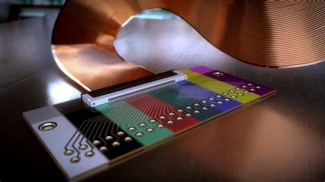
What is a PCB Prototype?
A printed circuit board (PCB) prototype is an early version or sample of a PCB design used for testing and evaluation before mass production. PCB Prototypes allow electronics designers and engineers to validate the functionality, performance, and manufacturability of a new PCB design.
PCB prototypes are fabricated using the same materials and processes as the final production version, but in smaller quantities – typically just a few boards. This enables issues to be identified and resolved, and the design to be refined and optimized iteratively before investing in the setup and components for volume manufacturing.
Why are PCB Prototypes Important?
PCB prototypes serve several critical functions in the electronics development process:
Design Validation
The primary purpose of a PCB prototype is to verify that the circuit design performs as intended. Prototypes allow designers to test the functionality and electrical characteristics of the board to ensure it meets the product requirements and specifications.
Debugging and Troubleshooting
Issues, bugs, and design flaws are often not apparent until a physical board is fabricated and powered on. PCB prototypes let engineers debug circuits, test components and interfaces, and identify any signal integrity, power integrity, EMI, thermal, or mechanical problems.
Design for Manufacturability
In addition to validating electrical performance, PCB prototypes also prove out the manufacturability of the board design. Aspects like component placement, routing, drill holes and vias, solder joints, and silkscreen must be evaluated on real hardware to verify they meet manufacturing constraints and will yield reliable, high-quality boards in volume production.
Compliance Testing
Any electronics product must pass a range of regulatory and compliance tests before it can legally be sold, including safety, RF emissions, susceptibility, and environmental. Functional prototypes that are equivalent to the final design are used for this compliance testing and certification.
Demonstration and Evaluation
PCB prototypes are also invaluable for demonstrating a new product to stakeholders and gathering feedback. Managers, clients, investors, or even focus groups can evaluate working prototypes to review the design and suggest improvements before finalizing the product.

PCB Prototyping Process
The process of taking a PCB from initial design to prototyped boards ready for testing involves several steps:
-
Schematic Capture – The first step is to create a schematic diagram of the circuit, defining the components and interconnections. This is typically done using electronic design automation (EDA) software.
-
Board Layout – Once the schematic is complete, the physical board layout is designed. Components are assigned to locations on the board and the copper traces that form the electrical connections are routed between them. The board shape, layer stackup, drill holes, and other mechanical features are also defined.
-
Design Rule Checks – The design software performs automated checks on the layout to verify it meets a comprehensive set of manufacturing and electrical rules, such as minimum trace widths and spacings, hole sizes, and clearances.
-
Simulation and Analysis – Next, various simulations can be run on the layout to analyze signal integrity, power integrity, EMI/EMC, and other characteristics. This isn’t a substitute for real-world testing, but can identify and correct many potential issues before committing to a prototype build.
-
Outputs Generation – When the PCB layout is finalized, the fabrication data is exported from the design software. This includes the Gerber files that define the copper patterns and drill data, component placement, test points, and additional drawings and documentation.
-
Prototype Fabrication – The PCB fabrication files are sent to a manufacturer that specializes in low-volume prototyping. They manufacture the bare circuit boards according to the design specifications. Depending on the complexity of the board, this can take anywhere from 1 day to 2 weeks typically.
-
Assembly – Once the bare PCBs are fabricated, the components are procured and assembled onto the board. This is usually done by machine, but for very low quantities the components may be hand soldered. The assembled PCBs are inspected and tested.
-
Testing and Rework – The assembled PCB prototypes are put through various functional, performance, and compliance tests to validate the design. Any problems are debugged and if necessary, the boards are reworked. The design may go through multiple prototype iterations before it is finalized for production.

Types of PCB Prototypes
There are a few different types of PCB prototypes that may be produced depending on the stage of the design and the specific testing requirements:
Visual Prototypes
Also known as a “looks-like” prototype, these are non-functional boards used to evaluate the visual appearance and mechanical form factor of the design. They have the final shape, thickness, and texture, with the components and graphics printed on the surface, but no real circuitry. These are useful for demonstrating the product at an early stage before investing in functional prototypes.
Proof-of-Concept Prototypes
An initial functional prototype used to quickly validate the basic circuit design and component selection, before finalizing the board layout. These may use larger than final components on a hand-wired or machine-routed board without the final form factor. PoC prototypes are used to test functionality and performance to identify any issues with the fundamental design approach.
Pre-Production Prototypes
These are fully-functional boards with the final PCB layout and bill of materials (BOM) that will be used for mass production. The purpose is to validate the production design and resolve any remaining issues before ramping up to volume manufacturing. Pre-production prototypes should perform identically to production boards and are used for final compliance testing and certification before the design is released for production.

PCB Prototype Manufacturing
Fabricating PCB prototypes requires specialized equipment and processes to produce high-quality boards in low volumes. Some key capabilities that differentiate PCB prototype manufacturers include:
Quick-Turn Production
PCB prototyping is extremely time sensitive, as it is often on the critical path for product development. Rapid prototype fabrication can be achieved with streamlined processes, automated equipment, and 24/7 operation. The fastest services can produce simple 2-layer boards in as little as 24 hours.
High Layer Count
Prototype PCBs are often complex boards with 8 or more layers, including high-density interconnect (HDI), blind and buried vias, and microvias. Prototype shops must have advanced multi-layer processing and laser drilling capabilities to fabricate these demanding designs.
Advanced Materials
Many PCB prototypes require specialized laminate materials, such as high-frequency Rogers, or thick-copper for high-power applications. Polyimide or high-temperature laminates may be specified for harsh environments. Prototyping with production materials ensures equivalent performance.
Finishes and Coatings
The final board finish, whether HASL, lead-free HASL, ENIG, or IAg, must be properly applied to the prototypes for good solderability. Conformal coatings for environmental protection and legend ink colors should also match the production boards.
Special Requirements
Capabilities such as controlled impedance, tight tolerances, and fine-pitch BGAs are often required for prototypes in high-speed digital, RF/wireless, and mobile device applications. The manufacturer should have experience with these technologies to deliver high-yield, reliable boards.
PCB Prototype Assembly
Assembling the PCB prototypes with components is a critical step that requires skilled technicians and specialized equipment. Key capabilities for PCB prototype assembly include:
Sourcing Components
The assembler must be able to source a wide variety of components, including obsolete or hard-to-find parts, in small quantities for prototypes. Strong supply chain relationships and inventory management are essential.
Machine Assembly
Automated assembly with pick-and-place machines and reflow ovens ensures consistent, reliable solder joints and placement accuracy, even for prototypes. Fine-pitch components like micro BGAs are placed more accurately by machine than by hand.
Hand Assembly
For very small quantities or large through-hole components, skilled technicians can hand solder parts onto the PCB. Prototypes often include oddform connectors, switches, and other parts that must be manually placed.
Mixed Technology
Many prototypes include both surface-mount and through-hole components on the same board. The assembler must be able to accommodate both technologies in the same process.
Inspection and Test
Assembled PCBs should be carefully inspected and tested, with AOI, X-ray, and electrical testing to verify proper assembly before being returned to the customer. Catching assembly errors early prevents costly debugging later.
Benefits of PCB Prototyping
Prototyping PCBs before full production provides a range of important benefits, including:
- Catching design errors and flaws early, before mass production
- Enabling faster debugging and troubleshooting of issues
- Allowing testing and validation of PCB functionality and performance
- Verifying manufacturability and optimizing the design for production
- Providing a proof-of-concept to demonstrate to stakeholders
- Accelerating time to market by validating the design in advance
Types of PCB Testing
PCB prototypes should undergo a range of tests to fully validate the design and identify any issues. Some key types of PCB testing include:
Power-On Testing
As soon as the board is received, a basic power-on test is performed to verify that it powers up safely without shorts or failures.
Electrical Testing
A series of tests to verify that electrical characteristics such as voltage levels, resistances, and capacitances match the expected values from design.
Functional Testing
The assembled PCB is tested under real-world operating conditions to verify that it functions and performs as intended in the end product.
Environmental Testing
Accelerated life tests that subject boards to thermal cycling, vibration, and shock to ensure field reliability and durability.
Compliance Testing
Certify that the PCB meets EMC, safety, and energy standards such as FCC, CE, and UL. More stringent testing may be required for specific industries such as aerospace, medical, or military.
PCB Prototype Costs and Lead Times
The cost and turnaround time for PCB prototypes depends on the complexity of the design and the volume required. Some general guidelines:
- Simple 2-layer boards can be fabricated in 1-2 days for around $100-200
- 4-layer boards typically take 3-5 days and cost $300-500
- Complex multilayer boards (8+) may take 1-2 weeks and cost $1000 or more
- Higher volumes (50+) reduce the per-board cost but increase overall cost and lead time
- Expedited services are available for a premium, at 2-3x normal cost
It is important to factor prototype costs and timelines into the overall product development budget and schedule. Trying to reduce prototyping to save time or money often results in preventable design issues and costly delays later.
FAQ
How many prototypes should I build?
It depends on the complexity of the design and the amount of debugging and testing anticipated. Three is a common recommendation: one for bench testing and debugging, one for compliance testing, and a spare.
Do I need to prototype every revision?
Not necessarily, minor revisions that don’t impact functionality or form factor may not need a prototype build. Major revisions with new features or components should always be prototyped.
Can I use different components for prototyping?
Yes, if equivalent components are unavailable in small quantities, substitutes can be used. But the final BOM should be prototyped before production to verify functionality and manufacturability.
What if my prototype doesn’t work?
This is actually the purpose of prototyping – to identify design issues. Debugging the root cause may uncover problems with component selection, signal integrity, software, or manufacturing. Rework and iterate the design, then prototype again.
How do I select a PCB prototype manufacturer?
Look for a shop with experience in your industry and technology. Check capabilities, certifications, and lead times. Get references from similar designs if possible.
In summary, PCB prototyping is a critical step in electronics product development that enables design validation and optimization prior to committing to full production. While it requires time and cost, prototyping done effectively significantly reduces risk and accelerates time-to-market. Choosing an experienced PCB prototype partner is key to getting reliable, fully-functional boards to keep the project moving forward.


Leave a Reply