What is a Presensitized PCB?
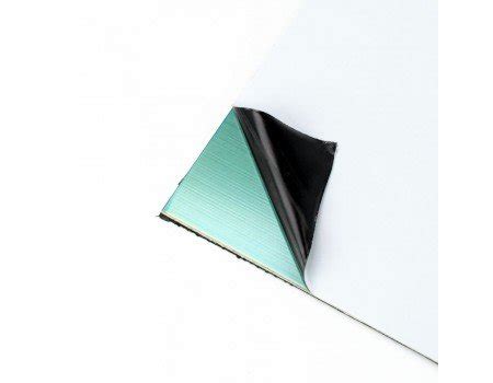
A presensitized PCB, also known as a photosensitive PCB or a pre-coated PCB, is a printed circuit board that has been coated with a light-sensitive material called photoresist. This coating allows for the creation of precise circuit patterns on the board through a process called photolithography. Presensitized PCBs have become increasingly popular in the electronics industry due to their ability to produce high-quality, complex circuit designs with excellent accuracy and repeatability.
Advantages of Presensitized PCBs
Presensitized PCBs offer several advantages over traditional PCB fabrication methods:
- High precision: The photolithography process used in presensitized PCBs allows for the creation of extremely precise circuit patterns with fine details and tight tolerances.
- Consistency: The pre-coating of photoresist ensures a consistent thickness and uniformity across the entire board, resulting in more reliable and repeatable circuit designs.
- Faster production: Presensitized PCBs can be processed more quickly than traditional PCBs, as the photoresist coating eliminates the need for manual resist application.
- Cost-effective: For high-volume production runs, presensitized PCBs can be more cost-effective than other PCB fabrication methods due to the streamlined manufacturing process.
How are Presensitized PCBs Manufactured?
The manufacturing process for presensitized PCBs involves several key steps:
- Substrate preparation: The PCB substrate, typically made of fiberglass or other insulating material, is cleaned and prepared for the photoresist coating.
- Photoresist application: The substrate is coated with a thin, uniform layer of photoresist material. This is usually done through a process called curtain coating or roller coating.
- Exposure: The coated PCB is then exposed to UV light through a photomask, which contains the desired circuit pattern. The UV light hardens the exposed areas of the photoresist, while the unexposed areas remain soluble.
- Development: The PCB is then placed in a developer solution, which removes the unexposed photoresist, leaving behind the hardened circuit pattern.
- Etching: The developed PCB undergoes an etching process, where the exposed copper areas are removed using a chemical etchant, leaving behind the desired circuit traces.
- Stripping and finishing: The remaining photoresist is stripped away, and the PCB undergoes final finishing processes, such as solder mask application and silkscreen printing.
Photoresist Types
There are two main types of photoresist used in presensitized PCBs:
- Positive photoresist: In this type, the areas exposed to UV light become soluble and are removed during development, while the unexposed areas remain intact. This results in a positive image of the circuit pattern.
- Negative photoresist: With negative photoresist, the exposed areas become insoluble and remain on the board after development, while the unexposed areas are removed. This creates a negative image of the circuit pattern.
The choice between positive and negative photoresist depends on factors such as the desired circuit design, manufacturing process, and cost considerations.

Designing for Presensitized PCBs
When designing a circuit for a presensitized PCB, there are several key considerations to keep in mind:
- Minimum feature size: The photolithography process used in presensitized PCBs has limitations in terms of the minimum feature size that can be reliably produced. Designers must ensure that their circuit patterns adhere to the manufacturer’s specifications for minimum trace width, spacing, and hole size.
- Photomask design: The photomask used in the exposure process must be carefully designed to ensure accurate transfer of the circuit pattern to the PCB. This includes considerations such as image polarity, alignment marks, and registration holes.
- Material selection: The choice of PCB substrate material and photoresist type can impact the performance and manufacturability of the final product. Designers should work closely with their PCB manufacturer to select the most appropriate materials for their application.
- Design for manufacturing (DFM): To ensure the best possible yield and reliability, designers should follow DFM guidelines when creating their circuit layouts. This includes adhering to recommended trace widths and spacings, avoiding sharp angles and abrupt changes in direction, and providing adequate clearance around holes and other features.
Design Software and File Formats
Most PCB design software packages support the creation of designs for presensitized PCBs. Some popular options include:
- Altium Designer
- Eagle PCB
- KiCad
- OrCAD
- Allegro PCB Designer
When submitting designs for manufacturing, the most common file formats used are Gerber files (RS-274X) and Excellon drill files. These file formats provide a standardized way of conveying the circuit pattern and drilling information to the PCB manufacturer.

Applications of Presensitized PCBs
Presensitized PCBs are used in a wide range of electronic applications, including:
- Consumer electronics: Smartphones, tablets, laptops, and other consumer devices rely on high-density, complex PCB designs that are well-suited to the presensitized manufacturing process.
- Automotive electronics: The demanding environment and reliability requirements of automotive electronics make presensitized PCBs an attractive option for applications such as engine control units, infotainment systems, and driver assistance systems.
- Medical devices: The high precision and consistency of presensitized PCBs are essential for medical device applications, where reliability and accuracy are critical.
- Aerospace and defense: The ability to produce complex, high-density circuit designs with tight tolerances makes presensitized PCBs well-suited for use in aerospace and defense applications, such as avionics systems and military communications equipment.
- Industrial automation: Presensitized PCBs are used in a variety of industrial automation applications, including process control systems, robotics, and machine vision systems.

Choosing a Presensitized PCB Manufacturer
When selecting a presensitized PCB manufacturer, there are several key factors to consider:
- Technical capabilities: Ensure that the manufacturer has the necessary equipment and expertise to produce PCBs that meet your design requirements, including minimum feature sizes, layer counts, and material specifications.
- Quality control: Look for a manufacturer with a robust quality control process, including automated optical inspection (AOI), X-ray inspection, and electrical testing to ensure the reliability and consistency of the finished product.
- Lead times: Consider the manufacturer’s typical lead times for prototyping and production runs, and ensure that they can meet your project timelines.
- Cost: Obtain quotes from multiple manufacturers and compare pricing, taking into account factors such as minimum order quantities, setup charges, and shipping costs.
- Customer support: Choose a manufacturer with responsive and knowledgeable customer support, who can provide guidance and assistance throughout the design and manufacturing process.
PCB Manufacturers Comparison
| Manufacturer | Minimum Feature Size | Maximum Layers | Lead Time (Prototype) | Lead Time (Production) |
|---|---|---|---|---|
| PCBWay | 3.5 mil (0.09 mm) | 16 | 24 hours | 3-5 days |
| JLCPCB | 3.5 mil (0.09 mm) | 16 | 24 hours | 3-5 days |
| ALLPCB | 3.9 mil (0.10 mm) | 28 | 24 hours | 3-5 days |
| PCBCart | 3 mil (0.08 mm) | 32 | 5 days | 10-15 days |
| Seeed Studio | 3.9 mil (0.10 mm) | 16 | 3 days | 7-10 days |
Note: Lead times and specifications may vary depending on the specific requirements of your project and the current market conditions. Always consult with the manufacturer for the most up-to-date information.
Frequently Asked Questions (FAQ)
-
What is the difference between a presensitized PCB and a standard PCB?
A presensitized PCB is pre-coated with a light-sensitive photoresist material, which allows for the creation of precise circuit patterns through a photolithography process. Standard PCBs do not have this pre-coating and require manual resist application during the manufacturing process. -
Can presensitized PCBs be used for prototyping?
Yes, presensitized PCBs can be used for prototyping. Many PCB manufacturers offer rapid prototyping services for presensitized PCBs, with lead times as short as 24 hours. -
Are there any limitations to the complexity of circuit designs that can be produced using presensitized PCBs?
Presensitized PCBs can accommodate complex, high-density circuit designs, but there are limitations in terms of the minimum feature sizes that can be reliably produced. Designers must work within the manufacturing capabilities of their chosen PCB supplier. -
How do I choose the right photoresist type for my presensitized PCB?
The choice between positive and negative photoresist depends on factors such as the desired circuit design, manufacturing process, and cost considerations. Consult with your PCB manufacturer to determine the most appropriate photoresist type for your project. -
What are the key considerations when designing a circuit for a presensitized PCB?
When designing a circuit for a presensitized PCB, key considerations include adhering to the manufacturer’s specifications for minimum feature sizes, designing an accurate photomask, selecting appropriate materials, and following design for manufacturing (DFM) guidelines to ensure the best possible yield and reliability.
In conclusion, presensitized PCBs offer a high-precision, consistent, and cost-effective solution for a wide range of electronic applications. By understanding the manufacturing process, design considerations, and key factors in choosing a manufacturer, designers can leverage the benefits of presensitized PCBs to create complex, reliable circuit designs that meet the demands of today’s electronic products.


Leave a Reply