What is PCBA Testing?
PCBA (Printed Circuit Board Assembly) testing is a crucial process in the manufacturing of electronic devices. It involves testing the assembled PCB to ensure that it functions as intended and meets the required specifications. PCBA testing is essential to identify any defects or issues in the PCB assembly process, such as short circuits, open circuits, incorrect component placement, or soldering defects.
Types of PCBA Tests
There are various types of PCBA tests that can be performed, depending on the complexity of the PCB and the requirements of the end product. Some of the common types of PCBA tests include:
- In-Circuit Testing (ICT)
- Flying Probe Testing
- Boundary Scan Testing
- Functional Testing
- Burn-in Testing
In-Circuit Testing (ICT)
In-Circuit Testing is a type of PCBA test that involves testing individual components on the PCB to ensure that they are functioning correctly. ICT is performed using a bed-of-nails fixture that makes contact with specific points on the PCB. The test system then applies stimuli to the components and measures their responses to determine if they are within the acceptable range.
| Advantages of ICT | Disadvantages of ICT |
|---|---|
| High fault coverage | Expensive fixture development |
| Fast test execution | Limited access to components |
| Automated testing | Potential damage to PCB |
Flying Probe Testing
Flying Probe Testing is a type of PCBA test that uses mobile probes to make contact with specific points on the PCB. Unlike ICT, Flying Probe Testing does not require a custom fixture, making it more flexible and cost-effective for low-volume production or prototype testing.
| Advantages of Flying Probe Testing | Disadvantages of Flying Probe Testing |
|---|---|
| No custom fixture required | Slower test execution compared to ICT |
| Flexible test coverage | Limited test coverage for complex PCBs |
| Ideal for low-volume production | Higher cost per test compared to ICT |
Boundary Scan Testing
Boundary Scan Testing is a type of PCBA test that uses the JTAG (Joint Test Action Group) interface to test the interconnections between components on the PCB. It involves using a boundary scan compliant device, such as a microprocessor or FPGA, to control and observe the signals at the component boundaries.
| Advantages of Boundary Scan Testing | Disadvantages of Boundary Scan Testing |
|---|---|
| Test coverage for complex PCBs | Requires JTAG compliant devices |
| No physical access required | Limited test coverage for analog components |
| Ideal for high-density PCBs | Additional design considerations for JTAG |
Functional Testing
Functional Testing is a type of PCBA test that involves testing the complete functionality of the assembled PCB. It is performed by applying input signals to the PCB and measuring the output signals to ensure that they meet the expected results. Functional Testing is often performed in conjunction with other types of PCBA tests to provide comprehensive test coverage.
| Advantages of Functional Testing | Disadvantages of Functional Testing |
|---|---|
| Tests the complete functionality of the PCB | Requires specialized test equipment |
| Ensures the PCB meets the end-product requirements | Time-consuming test development |
| Identifies issues not detected by other tests | May not detect all manufacturing defects |
Burn-in Testing
Burn-in Testing is a type of PCBA test that involves subjecting the assembled PCB to elevated temperatures and operating conditions for an extended period. The purpose of Burn-in Testing is to identify any early-life failures or defects that may not be detected by other types of PCBA tests.
| Advantages of Burn-in Testing | Disadvantages of Burn-in Testing |
|---|---|
| Identifies early-life failures | Time-consuming process |
| Ensures reliability of the PCB | Requires specialized equipment |
| Reduces warranty claims and field failures | Increased production costs |
PCBA Test Process
The PCBA test process typically involves the following steps:
- Test Plan Development
- Test Fixture Design and Fabrication
- Test Program Development
- PCB Assembly and Inspection
- PCBA Testing
- Failure Analysis and Repair
- Final Inspection and Packaging
Test Plan Development
The first step in the PCBA test process is to develop a comprehensive test plan. The test plan should define the types of tests to be performed, the test coverage requirements, and the acceptance criteria for each test. The test plan should also consider the specific requirements of the end product, such as environmental conditions, reliability, and safety standards.
Test Fixture Design and Fabrication
Based on the test plan, the next step is to design and fabricate the test fixtures required for each type of PCBA test. The test fixtures should be designed to provide reliable and repeatable contact with the PCB, while minimizing the risk of damage to the components. The test fixtures should also be designed to accommodate any variations in the PCB design, such as component placement or board thickness.
Test Program Development
The test program is the software that controls the test equipment and executes the PCBA tests. The test program should be developed based on the test plan and the specific requirements of each type of test. The test program should include the necessary test sequences, test parameters, and data logging capabilities to ensure accurate and reliable test results.
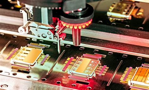
PCB Assembly and Inspection
Before the PCBA testing can begin, the PCB must be assembled and inspected to ensure that it meets the required specifications. The PCB assembly process typically involves the following steps:
- Solder Paste Application
- Component Placement
- Reflow Soldering
- Inspection and Rework
After the PCB assembly is complete, it should be inspected to ensure that all components are correctly placed and soldered, and that there are no visible defects or damage.
PCBA Testing
Once the PCB assembly is complete and inspected, the PCBA testing can begin. The specific types of tests to be performed will depend on the test plan and the requirements of the end product. The PCBA testing process typically involves the following steps:
- Test Fixture Setup
- Test Program Execution
- Data Analysis and Reporting
During the PCBA testing process, the test results should be carefully monitored and analyzed to identify any issues or defects. If any failures are detected, they should be documented and reported for further analysis and repair.
Failure Analysis and Repair
If any failures are detected during the PCBA testing process, the next step is to perform a failure analysis to determine the root cause of the issue. The failure analysis may involve visual inspection, X-ray inspection, or other diagnostic techniques to identify the specific component or area of the PCB that is causing the failure.
Once the root cause of the failure is identified, the PCB should be repaired or reworked as necessary to correct the issue. The repaired PCB should then be retested to ensure that the issue has been resolved and that the PCB meets the required specifications.
Final Inspection and Packaging
After the PCBA testing and any necessary repairs or rework are complete, the PCB should undergo a final inspection to ensure that it meets all the required specifications and quality standards. The final inspection may include visual inspection, functional testing, or other quality control measures.
Once the final inspection is complete, the PCB should be packaged and prepared for shipment to the customer or end-user. The packaging should be designed to protect the PCB from damage during transportation and storage, and should include any necessary documentation or labeling.

PCBA Test Equipment
There are various types of test equipment used in PCBA testing, depending on the specific requirements of each type of test. Some of the common types of PCBA test equipment include:
- In-Circuit Test (ICT) Systems
- Flying Probe Test Systems
- Boundary Scan Test Systems
- Functional Test Systems
- Burn-in Test Chambers
In-Circuit Test (ICT) Systems
In-Circuit Test (ICT) systems are used to perform in-circuit testing of individual components on the PCB. ICT systems typically consist of a bed-of-nails fixture that makes contact with specific points on the PCB, and a test system that applies stimuli to the components and measures their responses.
| Advantages of ICT Systems | Disadvantages of ICT Systems |
|---|---|
| High fault coverage | Expensive fixture development |
| Fast test execution | Limited access to components |
| Automated testing | Potential damage to PCB |
Flying Probe Test Systems
Flying Probe Test systems are used to perform flying probe testing of the PCB. Flying Probe Test systems use mobile probes to make contact with specific points on the PCB, and do not require a custom fixture. This makes them more flexible and cost-effective for low-volume production or prototype testing.
| Advantages of Flying Probe Test Systems | Disadvantages of Flying Probe Test Systems |
|---|---|
| No custom fixture required | Slower test execution compared to ICT |
| Flexible test coverage | Limited test coverage for complex PCBs |
| Ideal for low-volume production | Higher cost per test compared to ICT |
Boundary Scan Test Systems
Boundary Scan Test systems are used to perform boundary scan testing of the interconnections between components on the PCB. Boundary Scan Test systems use a boundary scan compliant device, such as a microprocessor or FPGA, to control and observe the signals at the component boundaries.
| Advantages of Boundary Scan Test Systems | Disadvantages of Boundary Scan Test Systems |
|---|---|
| Test coverage for complex PCBs | Requires JTAG compliant devices |
| No physical access required | Limited test coverage for analog components |
| Ideal for high-density PCBs | Additional design considerations for JTAG |
Functional Test Systems
Functional Test systems are used to perform functional testing of the complete functionality of the assembled PCB. Functional Test systems apply input signals to the PCB and measure the output signals to ensure that they meet the expected results.
| Advantages of Functional Test Systems | Disadvantages of Functional Test Systems |
|---|---|
| Tests the complete functionality of the PCB | Requires specialized test equipment |
| Ensures the PCB meets the end-product requirements | Time-consuming test development |
| Identifies issues not detected by other tests | May not detect all manufacturing defects |
Burn-in Test Chambers
Burn-in Test chambers are used to perform burn-in testing of the assembled PCB. Burn-in Test chambers subject the PCB to elevated temperatures and operating conditions for an extended period, to identify any early-life failures or defects.
| Advantages of Burn-in Test Chambers | Disadvantages of Burn-in Test Chambers |
|---|---|
| Identifies early-life failures | Time-consuming process |
| Ensures reliability of the PCB | Requires specialized equipment |
| Reduces warranty claims and field failures | Increased production costs |

PCBA Test Standards and Regulations
PCBA testing is subject to various standards and regulations, depending on the specific industry and application of the end product. Some of the common PCBA test standards and regulations include:
- IPC-A-610: Acceptability of Electronic Assemblies
- IPC-7711/7721: Rework, Modification and Repair of Electronic Assemblies
- IPC-9252: Requirements for Electrical Testing of Unpopulated Printed Boards
- J-STD-001: Requirements for Soldered Electrical and Electronic Assemblies
- MIL-STD-202: Test Methods for Electronic and Electrical Component Parts
These standards and regulations provide guidelines for the acceptable quality and reliability of PCB assemblies, as well as the methods and procedures for testing and inspection.

FAQ
1. What is the difference between ICT and Flying Probe Testing?
ICT (In-Circuit Testing) requires a custom test fixture to make contact with specific points on the PCB, while Flying Probe Testing uses mobile probes to make contact with the PCB and does not require a custom fixture. ICT is faster and provides higher fault coverage, but is more expensive and may cause damage to the PCB. Flying Probe Testing is more flexible and cost-effective for low-volume production or prototype testing, but is slower and may have limited test coverage for complex PCBs.
2. What is Boundary Scan Testing?
Boundary Scan Testing is a type of PCBA test that uses the JTAG (Joint Test Action Group) interface to test the interconnections between components on the PCB. It involves using a boundary scan compliant device, such as a microprocessor or FPGA, to control and observe the signals at the component boundaries. Boundary Scan Testing provides test coverage for complex PCBs and does not require physical access to the components, but requires JTAG compliant devices and may have limited test coverage for analog components.
3. What is Functional Testing?
Functional Testing is a type of PCBA test that involves testing the complete functionality of the assembled PCB. It is performed by applying input signals to the PCB and measuring the output signals to ensure that they meet the expected results. Functional Testing ensures that the PCB meets the end-product requirements and identifies issues not detected by other tests, but requires specialized test equipment and may not detect all manufacturing defects.
4. What is Burn-in Testing?
Burn-in Testing is a type of PCBA test that involves subjecting the assembled PCB to elevated temperatures and operating conditions for an extended period. The purpose of Burn-in Testing is to identify any early-life failures or defects that may not be detected by other types of PCBA tests. Burn-in Testing ensures the reliability of the PCB and reduces warranty claims and field failures, but is a time-consuming process that requires specialized equipment and increases production costs.
5. What are the common PCBA test standards and regulations?
Some of the common PCBA test standards and regulations include IPC-A-610 (Acceptability of Electronic Assemblies), IPC-7711/7721 (Rework, Modification and Repair of Electronic Assemblies), IPC-9252 (Requirements for Electrical Testing of Unpopulated Printed Boards), J-STD-001 (Requirements for Soldered Electrical and Electronic Assemblies), and MIL-STD-202 (Test Methods for Electronic and Electrical Component Parts). These standards and regulations provide guidelines for the acceptable quality and reliability of PCB assemblies, as well as the methods and procedures for testing and inspection.


Leave a Reply