What is a PCB Via?
A PCB (Printed Circuit Board) via is a small hole drilled through the board to allow electrical connections between different layers of the PCB. Vias are essential components in multi-layer PCBs, enabling the routing of signals and power between layers, which is crucial for complex electronic designs.
Types of PCB Vias
There are several types of PCB vias, each with its own characteristics and applications:
Through-hole Vias
Through-hole vias are the most common type of via. They are drilled through the entire thickness of the PCB and are typically plated with a conductive material, such as copper, to create an electrical connection between layers.
Blind Vias
Blind vias are drilled from one side of the PCB and terminate at an inner layer, rather than passing through the entire board. They are used to connect an outer layer to one or more inner layers, but not to the opposite side of the board.
Buried Vias
Buried vias are located entirely within the inner layers of a PCB and do not connect to either outer layer. They are used to connect two or more inner layers without being visible on the surface of the board.
Micro Vias
Micro vias are small, laser-drilled vias with diameters typically less than 0.15mm (6 mils). They are used in high-density interconnect (HDI) PCBs to create fine-pitch connections between layers.

PCB Via Size Considerations
When designing a PCB, it’s essential to choose the appropriate via size to ensure proper electrical connections, manufacturability, and reliability. Several factors influence the choice of via size:
Current Carrying Capacity
The current carrying capacity of a via depends on its cross-sectional area. Larger vias can handle higher currents without overheating or causing voltage drops. The table below shows the approximate current carrying capacity for various via sizes:
| Via Diameter (mm) | Current Carrying Capacity (A) |
|---|---|
| 0.2 | 0.5 |
| 0.3 | 1.0 |
| 0.4 | 1.5 |
| 0.5 | 2.0 |
| 0.6 | 2.5 |
| 0.8 | 3.5 |
| 1.0 | 4.5 |
Manufacturing Constraints
The minimum via size is limited by the manufacturing capabilities of the PCB fabrication process. Smaller vias require more precise drilling and plating, which can increase manufacturing costs. The table below shows typical via sizes for different PCB classes:
| PCB Class | Minimum Via Diameter (mm) | Typical Via Diameter (mm) |
|---|---|---|
| Class 1 | 0.5 | 0.8 – 1.0 |
| Class 2 | 0.3 | 0.5 – 0.8 |
| Class 3 | 0.2 | 0.3 – 0.5 |
| Class 4 | 0.1 | 0.2 – 0.3 |
Signal Integrity
Via size can impact signal integrity, especially at high frequencies. Smaller vias have lower inductance and capacitance, which can help reduce signal reflections and crosstalk. However, smaller vias also have higher resistance, which can lead to signal attenuation.
Thermal Management
Vias can be used for thermal management by conducting heat away from components and into the PCB substrate or heatsinks. Larger vias have better thermal conductivity and can more effectively dissipate heat.

PCB Via Size Calculation
To calculate the appropriate via size for a given application, designers must consider factors such as current carrying capacity, manufacturing constraints, and signal integrity. The following equations can be used to estimate via dimensions:
Via Diameter
The via diameter (D) can be calculated based on the desired current carrying capacity (I) and the maximum allowable current density (J) for the via plating material:
D = sqrt(4 * I / (π * J))
For example, if a via needs to carry 1A of current and the maximum allowable current density for copper plating is 100A/mm², the minimum via diameter would be:
D = sqrt(4 * 1A / (π * 100A/mm²)) ≈ 0.113mm
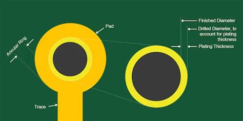
Via Pad Size
The via pad size (P) should be larger than the via diameter to allow for proper plating and to provide sufficient annular ring for reliable connections. A common rule of thumb is to make the pad diameter 0.25mm larger than the via diameter:
P = D + 0.25mm
For the previous example, with a via diameter of 0.113mm, the recommended pad size would be:
P = 0.113mm + 0.25mm = 0.363mm

PCB Via Size Standards
Several industry standards provide guidelines for PCB via sizes and their associated pad sizes. Some common standards include:
- IPC-2221: Generic Standard on Printed Board Design
- IPC-6012: Qualification and Performance Specification for Rigid Printed Boards
- IPC-7351: Generic Requirements for Surface Mount Design and Land Pattern Standards
These standards offer recommendations for minimum via sizes, pad sizes, and clearances based on the PCB class and the specific application requirements.
Frequently Asked Questions (FAQ)
1. What is the smallest possible via size?
The smallest possible via size depends on the PCB manufacturing capabilities. For most standard PCB fabrication processes, the minimum via diameter is around 0.1mm (4 mils). However, advanced HDI processes can achieve via sizes as small as 0.05mm (2 mils) or less.
2. How do I choose the right via size for my PCB design?
When choosing a via size, consider factors such as the required current carrying capacity, manufacturability, signal integrity, and thermal management. Consult with your PCB manufacturer to determine their capabilities and recommendations for your specific application.
3. Can vias be used for heat dissipation?
Yes, vias can be used for heat dissipation by conducting heat away from components and into the PCB substrate or heatsinks. Larger vias and thermal via arrays are more effective at transferring heat.
4. What is the difference between a through-hole via and a blind via?
A through-hole via passes through the entire thickness of the PCB, connecting layers on both sides of the board. A blind via, on the other hand, is drilled from one side of the PCB and terminates at an inner layer, connecting an outer layer to one or more inner layers, but not to the opposite side of the board.
5. How do vias affect signal integrity in high-speed PCB designs?
Vias can impact signal integrity in high-speed PCB designs by introducing discontinuities, reflections, and crosstalk. Smaller vias generally have lower inductance and capacitance, which can help minimize these effects. However, smaller vias also have higher resistance, which can lead to signal attenuation. Careful via placement, sizing, and optimization are essential for maintaining signal integrity in high-speed designs.
Conclusion
PCB via size is a critical aspect of PCB design, affecting electrical performance, manufacturability, and reliability. By understanding the different types of vias, their size considerations, and the relevant industry standards, designers can make informed decisions when selecting via sizes for their PCB projects. Careful via sizing and optimization can help ensure proper electrical connections, minimize signal integrity issues, and improve overall PCB performance.


Leave a Reply