What is PCB Trace Thickness?
PCB trace thickness refers to the thickness of the copper traces on a printed circuit board. These traces are the conductive paths that carry electrical signals and power between components on the board. The thickness of these traces is typically measured in ounces of copper per square foot (oz/ft²) or in microns (μm).
Common PCB Trace Thickness Values
| Thickness (oz/ft²) | Thickness (μm) |
|---|---|
| 0.5 oz/ft² | 17.5 μm |
| 1 oz/ft² | 35 μm |
| 2 oz/ft² | 70 μm |
| 3 oz/ft² | 105 μm |
| 4 oz/ft² | 140 μm |
Importance of PCB Trace Thickness
Current-Carrying Capacity
The thickness of PCB traces directly affects their current-carrying capacity. Thicker traces can handle higher currents without overheating or experiencing excessive voltage drop. This is particularly important for power traces and high-current applications.
Signal Integrity
PCB trace thickness also impacts signal integrity. Thinner traces have higher resistance, which can lead to signal degradation and increased noise. On the other hand, thicker traces have lower resistance and can maintain signal integrity over longer distances.
Manufacturing Considerations
The choice of PCB trace thickness also affects the manufacturing process. Thinner traces require more precise etching and are more susceptible to manufacturing defects. Thicker traces are easier to manufacture but may increase the overall cost of the PCB.

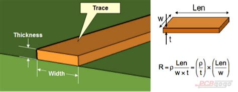
Calculating PCB Trace Thickness
To determine the appropriate PCB trace thickness for your design, you need to consider factors such as the required current-carrying capacity, the maximum allowable temperature rise, and the PCB material properties. Here are some methods for calculating PCB trace thickness:
IPC-2221 Standard
The IPC-2221 standard provides guidelines for calculating PCB trace thickness based on the required current and the maximum allowable temperature rise. The standard offers charts and formulas to help designers determine the appropriate trace width and thickness for their specific application.
Online Calculators
There are numerous online calculators available that can help you determine the appropriate PCB trace thickness for your design. These calculators typically require inputs such as the desired current, the maximum allowable temperature rise, and the PCB material properties.

Best Practices for PCB Trace Thickness
Consider Current Requirements
When designing your PCB, consider the current requirements of each trace. Power traces and high-current signals should have thicker traces to ensure adequate current-carrying capacity and minimize voltage drop.
Use Appropriate Trace Widths
In addition to trace thickness, trace width also plays a role in current-carrying capacity and signal integrity. Use appropriate trace widths based on the current requirements and the available space on the PCB.
Optimize for Manufacturing
Consider the capabilities of your PCB manufacturer when selecting trace thickness. Thinner traces may require more advanced manufacturing processes and increase the cost of the PCB. Strike a balance between performance and manufacturability.
Conduct Thermal Analysis
Perform thermal analysis to ensure that your PCB traces can handle the expected current without excessive temperature rise. This is particularly important for high-power applications and dense PCB layouts.

FAQ
1. What is the most common PCB trace thickness?
The most common PCB trace thickness is 1 oz/ft² (35 μm). This thickness provides a good balance between current-carrying capacity, signal integrity, and manufacturability for most applications.
2. Can I mix different trace thicknesses on the same PCB?
Yes, you can use different trace thicknesses on the same PCB. This is often done to optimize current-carrying capacity and signal integrity for specific traces while minimizing overall cost.
3. How does PCB trace thickness affect impedance?
PCB trace thickness affects impedance by changing the cross-sectional area of the trace. Thicker traces have lower impedance, while thinner traces have higher impedance. This relationship is important to consider when designing high-speed or impedance-controlled traces.
4. What happens if PCB traces are too thin?
If PCB traces are too thin, they may not be able to handle the required current, leading to overheating and potential failure. Thin traces also have higher resistance, which can cause signal degradation and increased noise.
5. Can I increase PCB trace thickness after manufacturing?
No, once a PCB has been manufactured, the trace thickness cannot be increased. If you need to increase the current-carrying capacity of a trace, you would need to redesign the PCB with thicker traces and have it re-manufactured.
Conclusion
PCB trace thickness is a critical factor in the design and manufacturing of printed circuit boards. It affects current-carrying capacity, signal integrity, and manufacturing considerations. By understanding the importance of trace thickness, using appropriate calculation methods, and following best practices, you can optimize your PCB design for performance, reliability, and cost-effectiveness.
When designing your PCB, consider the current requirements of each trace, use appropriate trace widths, optimize for manufacturing, and conduct thermal analysis to ensure proper performance. By taking a comprehensive approach to PCB trace thickness, you can create high-quality, reliable PCBs that meet the demands of your specific application.


Leave a Reply