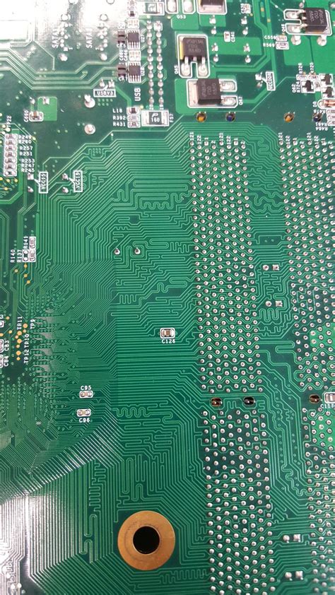
What are PCB Traces?
PCB traces are thin copper lines that are etched or printed onto the surface of a PCB. They serve as the electrical pathways that allow signals and power to flow between various components such as resistors, capacitors, integrated circuits (ICs), and connectors. The width, thickness, and spacing of these traces are critical factors in determining the electrical characteristics and signal integrity of the PCB.
Types of PCB Traces
There are several types of PCB traces, each serving a specific purpose:
-
Signal Traces: These traces carry electrical signals between components on the PCB. They are designed to maintain signal integrity and minimize noise and interference.
-
Power Traces: These traces are used to distribute power from the power source to various components on the PCB. They are typically wider than signal traces to handle higher currents.
-
Ground Traces: These traces provide a common ground reference for the components on the PCB. They help to reduce noise and ensure stable operation of the circuit.
-
Differential Pairs: These are pairs of traces that carry differential signals, such as high-speed digital signals or low-voltage differential signaling (LVDS). They are carefully routed to maintain a constant spacing and minimize crosstalk.
Importance of PCB Traces
PCB traces are essential for the proper functioning and performance of electronic devices. Here are some key reasons why PCB traces are crucial:
Signal Integrity
One of the primary goals of PCB design is to ensure signal integrity. Signal integrity refers to the ability of the PCB to maintain the quality and fidelity of the electrical signals as they travel through the traces. Poor signal integrity can lead to signal distortion, noise, crosstalk, and other issues that can negatively impact the performance of the device.
PCB traces play a vital role in maintaining signal integrity. The design of the traces, including their width, thickness, spacing, and routing, can significantly affect the signal quality. For example, traces that are too thin or too close together can result in increased resistance and capacitance, leading to signal degradation. On the other hand, properly designed traces can minimize signal reflections, reduce crosstalk, and ensure reliable signal transmission.
Power Distribution
Another important function of PCB traces is power distribution. The power traces on a PCB are responsible for delivering the required power from the power source to the various components on the board. Proper power distribution is essential for the stable and reliable operation of the device.
The design of power traces involves considerations such as current-carrying capacity, voltage drop, and thermal management. The width of the power traces must be sufficient to handle the expected current flow without excessive voltage drop or overheating. Additionally, the placement and routing of power traces should be optimized to minimize electromagnetic interference (EMI) and ensure a clean power supply to the components.
Electromagnetic Compatibility (EMC)
PCB traces can also impact the electromagnetic compatibility (EMC) of the device. EMC refers to the ability of the device to operate properly in the presence of electromagnetic interference (EMI) and to not generate excessive EMI that can affect other devices.
The layout and routing of PCB traces can have a significant effect on EMC. Traces that are not properly designed or routed can act as antennas, radiating EMI and causing interference with other devices. On the other hand, careful design techniques such as proper grounding, shielding, and filtering can help mitigate EMI and ensure compliance with EMC regulations.
Manufacturing Considerations
PCB traces also play a role in the manufacturability and reliability of the PCB. The design of the traces must take into account the manufacturing processes and limitations to ensure that the PCB can be efficiently and reliably produced.
For example, the width and spacing of the traces must be compatible with the etching or printing processes used in PCB fabrication. The traces must also be designed to withstand the thermal and mechanical stresses encountered during assembly and operation. Proper design practices, such as providing adequate clearances and using appropriate trace geometries, can help improve the manufacturability and reliability of the PCB.

PCB Trace Design Considerations
Designing PCB traces requires careful consideration of various factors to ensure optimal performance and reliability. Here are some key design considerations for PCB traces:
Trace Width and Thickness
The width and thickness of PCB traces are critical parameters that affect their electrical characteristics and current-carrying capacity. The trace width determines the resistance of the trace, with wider traces having lower resistance and higher current-carrying capacity. The trace thickness, on the other hand, affects the cross-sectional area of the trace and its ability to handle higher currents without excessive heating.
When designing PCB traces, it is important to select appropriate trace widths and thicknesses based on the expected current flow and the desired electrical characteristics. The IPC-2221 standard provides guidelines for determining the minimum trace width and thickness based on factors such as the current requirement, temperature rise, and copper weight.
| Current (A) | Trace Width (mm) | Trace Thickness (oz) |
|---|---|---|
| 0.5 | 0.2 | 1 |
| 1.0 | 0.3 | 1 |
| 2.0 | 0.6 | 2 |
| 3.0 | 0.9 | 2 |
| 5.0 | 1.5 | 3 |
Table 1: Example trace width and thickness guidelines based on current requirements.
Trace Spacing and Clearance
The spacing between PCB traces and the clearance between traces and other features on the PCB are important design considerations. Proper spacing and clearance help to minimize crosstalk, reduce EMI, and ensure manufacturability.
The spacing between traces depends on factors such as the signal frequency, voltage level, and the dielectric constant of the PCB material. High-speed signals require greater spacing to minimize crosstalk, while high-voltage traces need increased clearance to prevent arcing or breakdown.
The IPC-2221 standard provides recommendations for minimum trace spacing and clearance based on factors such as the voltage level, signal frequency, and PCB material.
| Voltage (V) | Minimum Spacing (mm) |
|---|---|
| 0-50 | 0.1 |
| 50-100 | 0.2 |
| 100-150 | 0.3 |
| 150-300 | 0.6 |
| 300-500 | 1.0 |
Table 2: Example minimum trace spacing guidelines based on voltage levels.
Trace Routing
The routing of PCB traces is a critical aspect of PCB design. Proper trace routing helps to minimize signal integrity issues, reduce EMI, and optimize the overall performance of the PCB.
When routing traces, it is important to consider factors such as signal integrity, crosstalk, and EMI. Traces should be routed as directly as possible to minimize signal reflections and delays. In high-speed designs, controlled impedance routing techniques, such as microstrip or stripline, may be used to maintain consistent impedance along the trace length.
Other routing considerations include avoiding sharp corners or acute angles, which can cause signal reflections, and providing adequate spacing between traces to minimize crosstalk. Ground planes and power planes should also be strategically placed to provide a low-impedance return path for signals and to minimize EMI.
Termination and Impedance Matching
Termination and impedance matching are important techniques used to ensure signal integrity in high-speed PCB designs. Termination refers to the practice of adding resistors or other components at the end of a trace to absorb or reflect signal energy and prevent reflections.
Impedance matching involves designing the PCB traces to have a characteristic impedance that matches the impedance of the source and load devices. This helps to minimize signal reflections and ensure efficient power transfer.
There are various termination and impedance matching techniques, such as series termination, parallel termination, and differential termination. The choice of termination and impedance matching depends on factors such as the signal frequency, trace length, and the characteristics of the source and load devices.
| Termination Type | Description |
|---|---|
| Series | Resistor placed in series with the signal trace |
| Parallel | Resistor placed in parallel with the signal trace |
| Differential | Resistors placed at the end of differential pair traces |
| AC | Capacitor placed in series with the signal trace |
| Thévenin | Combination of series and parallel resistors |
Table 3: Common termination techniques used in PCB design.

Best Practices for PCB Trace Design
To optimize the performance and reliability of PCB traces, consider the following best practices:
-
Follow industry standards: Adhere to industry standards such as IPC-2221 for trace width, thickness, spacing, and clearance guidelines.
-
Use appropriate trace geometries: Use appropriate trace geometries, such as rounded corners and smooth transitions, to minimize signal reflections and improve manufacturability.
-
Minimize trace length: Keep traces as short as possible to minimize signal delays and reduce the risk of signal integrity issues.
-
Provide adequate grounding: Use ground planes and strategically placed ground traces to provide a low-impedance return path for signals and minimize EMI.
-
Use controlled impedance routing: Employ controlled impedance routing techniques, such as microstrip or stripline, for high-speed signals to maintain consistent impedance along the trace length.
-
Avoid crosstalk: Provide adequate spacing between traces and use techniques such as guard traces or ground shielding to minimize crosstalk.
-
Consider thermal management: Ensure that power traces are sufficiently wide to handle the expected current flow without excessive heating.
-
Perform signal integrity simulations: Use signal integrity simulation tools to analyze and optimize the PCB traces for signal quality and performance.
-
Collaborate with PCB manufacturers: Work closely with PCB manufacturers to ensure that the trace design is compatible with their manufacturing processes and capabilities.

Frequently Asked Questions (FAQ)
-
What is the difference between a signal trace and a power trace?
Signal traces are used to carry electrical signals between components, while power traces are used to distribute power from the power source to various components on the PCB. Power traces are typically wider than signal traces to handle higher currents. -
How does trace width affect the electrical characteristics of a PCB trace?
The width of a PCB trace affects its resistance and current-carrying capacity. Wider traces have lower resistance and can handle higher currents without excessive voltage drop or heating. The appropriate trace width is determined based on factors such as the expected current flow and the desired electrical characteristics. -
What is controlled impedance routing, and why is it important?
Controlled impedance routing refers to techniques used to maintain consistent impedance along the length of a PCB trace. It is important for high-speed signals to ensure signal integrity and minimize reflections. Techniques such as microstrip or stripline routing are commonly used for controlled impedance routing. -
How can crosstalk be minimized in PCB trace design?
Crosstalk can be minimized by providing adequate spacing between traces, especially for high-speed signals. Other techniques include using guard traces or ground shielding to isolate sensitive traces from potential sources of crosstalk. Proper routing and placement of traces can also help reduce crosstalk. -
Why is it important to collaborate with PCB manufacturers during the trace design process?
Collaborating with PCB manufacturers is important to ensure that the trace design is compatible with their manufacturing processes and capabilities. PCB manufacturers can provide valuable insights and recommendations based on their experience and expertise. This collaboration helps to optimize the design for manufacturability, reliability, and cost-effectiveness.
Conclusion
PCB traces are the backbone of printed circuit boards, enabling the flow of electrical signals and power between components. The importance of PCB traces cannot be overstated, as they directly impact the performance, reliability, and electromagnetic compatibility of electronic devices.
Designing PCB traces requires careful consideration of various factors, including trace width and thickness, spacing and clearance, routing, termination, and impedance matching. Following industry standards, best practices, and collaborating with PCB manufacturers are essential for optimizing the design and ensuring the success of the PCB.
By understanding the importance of PCB traces and applying the principles and techniques discussed in this article, designers can create robust and high-performance PCBs that meet the demanding requirements of modern electronic devices.


Leave a Reply