Understanding RF Interference and Coupling Mechanisms
Radio frequency interference (RFI) refers to unwanted high frequency signals that can disrupt normal circuit operation. As the number of RF emitting devices like smartphones, Bluetooth accessories, and IoT devices continues to proliferate, RFI is an increasing concern for audio designers.
There are several ways that RF energy can couple into an audio circuit:
- Conducted – RF signals can enter the circuit directly through power supply lines, ground connections, and signal traces
- Radiated – RF fields can induce currents in PCB traces, component leads, and cables, especially those that form resonant antennas at the interfering frequency
- Capacitive/inductive coupling – Stray Capacitance or mutual inductance can couple RF energy between adjacent conductors
Minimizing the effects of RFI requires addressing all potential coupling paths through smart circuit design and PCB layout.
Optimizing Power Supply Filtering and Decoupling
Conducted RF interference on power rails is a common issue in audio circuits. To prevent RF noise from reaching sensitive amplifier stages:
- Use ferrite beads or dedicated RF chokes in series with power inputs to block high frequencies
- Place decoupling capacitors as close as possible to IC power pins and use multiple capacitors in parallel to provide low impedance across a wide frequency range (see table)
- Use power planes instead of traces to minimize inductance
- Implement separate analog and digital power rails with filtering at each domain crossing
| Capacitor Value | Effective Freq Range |
|---|---|
| 0.1uF | 10MHz – 100MHz |
| 1nF | 100MHz – 1GHz |
| 10pF | > 1GHz |
Table 1 – Recommended Decoupling Capacitor Values

Signal Trace Routing and Termination
Proper signal routing is critical to minimizing radiated and coupled RF interference:
- Keep sensitive analog signal traces as short as possible and avoid routing near noisy digital lines or connectors
- For differential signaling, use tightly coupled traces with equal length to maximize common-mode rejection
- Avoid routing traces parallel to board edges which can act as antennas
- Terminate transmission lines at the receiver with their characteristic impedance to prevent reflections
- Use guard rings or via fences around sensitive traces to provide shielding

Grounding and Shielding Techniques
A low-impedance, well-defined ground system is the foundation of RF Immunity. Key grounding approaches include:
- Use ground planes instead of traces to lower impedance and provide shielding
- Implement a star topology for ground connections to avoid creating loops
- Designate a single reference point for 0V
- Connect analog and digital ground planes at a single point beneath ADCs/DACs
- Isolate power and signal ground with ferrite beads in series
- For two layer boards without dedicated planes, use gridded power/ground pours
In addition to planes, physical shields can block radiated RF fields:
- Enclose sensitive circuitry in grounded metal cans soldered to the PCB
- Use shielded connectors and cables, with 360° termination of the shield conductor
- Apply conductive coatings like copper tape to the inside of plastic housings

Component Selection and Placement
Thoughtful component choice and placement also plays an important role in RF immunity:
- Select amplifier ICs with built-in RFI rejection features like input filtering
- Minimize package inductance by using surface mount components when possible
- Avoid stacking components which increases parasitic coupling
- Place decoupling capacitors as close as possible to device pins
- Provide good heatsinking to minimize thermal-induced offsets, especially with high gain stages
Minimizing Sensitive Trace Areas
RF interference is often coupled into a circuit through stray capacitance between PCB traces and other conductors. To minimize this effect:
- Keep loop areas small to avoid forming efficient antennas
- Route high impedance traces like amplifier inputs on inner layers between power and ground planes when possible
- Avoid suspended traces that are more susceptible to capacitive coupling
| Trace Width (mm) | 50Ω Microstrip Impedance (Ω) |
|---|---|
| 0.1 | 122 |
| 0.5 | 77 |
| 1 | 59 |
| 2 | 44 |
Table 2 – Approximate trace widths for 50Ω microstrip on 1.6mm FR4
Spread Spectrum Clocking
Many mixed-signal audio ICs include switching regulators and digital control circuitry that can generate noise at fixed frequencies. If this noise couples into analog circuits, it may mix with RF interference and fold back into the audio band.
One mitigation technique is spread spectrum clocking (SSC), where the clock frequency is intentionally modulated over a small range. This spreads the regulator noise over a wider bandwidth, reducing the energy at any one frequency. Some audio ICs have built-in SSC capability that can be enabled if RFI issues are encountered.
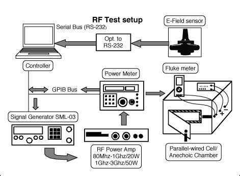
Testing and Verification
Comprehensive testing is required to verify the RF immunity of an audio design. Considerations include:
- Testing with real-world interference sources like phones and two-way radios in addition to lab generators
- Monitoring power rails with a spectrum analyzer to check for coupled spurs
- Measuring audio performance in an anechoic chamber to quantify shielding effectiveness
- Validating operation over temperature to check for thermal effects on offset/distortion
It’s important to leave sufficient time in the development schedule for thorough RFI testing and any necessary design revisions.
Frequently Asked Questions
What is the most important factor for achieving good RF immunity?
Maintaining a low-impedance, properly decoupled power distribution system is arguably the single most important aspect of RF immune design. Preventing conducted interference on the power rails stops RF energy at the source before it can couple into other circuits.
Do I need to worry about RFI if my product doesn’t have any wireless functionality?
Yes, all electronic devices can be affected by ambient RF fields from external sources like radio transmitters and cell towers. While products with intentional radiators like Bluetooth or WiFi may be more susceptible, RFI should be considered in any audio design.
Can software be used to improve RF immunity?
While software alone cannot block RF interference, clever coding can help in some cases. For example, using a “guard” time period without audio output immediately after enabling a power amplifier can prevent audible artifacts from the amplifier stabilizing after turn-on.
What is the best PCB material for reducing RFI?
FR-4 is sufficient for most audio applications, but using higher-quality laminates with lower dissipation factor can help reduce signal loss and attenuation at high frequencies. In very sensitive designs, specialized materials like Rogers 4350B may be used near RF components.
How much does PCB layout affect the cost of an audio product?
Implementing good layout techniques like short traces, solid ground planes, and filtered power rails may increase the size and layer count of a PCB relative to a quick-and-dirty design. However, this additional up-front cost is usually minor compared to the potential cost of dealing with RFI issues later in the development cycle or after production. Investing in a solid board layout is almost always worthwhile for a successful, EMC-compliant audio product.
Conclusion
Achieving reliable RF immunity in high-performance audio circuits requires a multi-faceted approach encompassing filtering, grounding, shielding, and layout best practices. By understanding common RFI coupling mechanisms and implementing the techniques described in this article, designers can realize audio amplifiers that deliver pristine sound quality even in hostile RF environments. While careful PCB design is not always the simplest or cheapest approach, it is essential to crafting audio products that meet the ever-increasing expectations of today’s consumers.


Leave a Reply