What is PCB Drilling?
PCB drilling is the process of creating holes in a printed circuit board to accommodate electronic components and establish electrical connections between layers. These holes, also known as vias, serve as conduits for electrical signals to travel through the board, enabling the functioning of the electronic device.
The drilling process is crucial in PCB manufacturing as it ensures the accurate placement of components and the proper functioning of the circuit. The holes created during drilling must be precise in terms of size, location, and depth to maintain the integrity of the PCB and prevent any electrical issues.
Types of PCB Drilling
There are several types of PCB drilling methods used in the manufacturing process. Each method has its advantages and is suited for specific applications. Let’s explore the main types of PCB drilling:
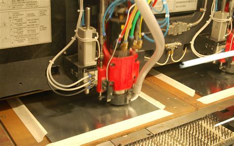
Mechanical Drilling
Mechanical drilling is the most common method used in PCB manufacturing. It involves using a drill bit to create holes in the PCB substrate. The drill bits are typically made of carbide or high-speed steel and come in various sizes to accommodate different hole diameters.
Advantages of mechanical drilling:
– Cost-effective for large-scale production
– Suitable for a wide range of hole sizes
– High drilling speed
Disadvantages of mechanical drilling:
– Limited precision compared to other methods
– Potential for drill bit wear and breakage
– Requires frequent tool changes for different hole sizes
Laser Drilling
Laser drilling uses a focused laser beam to create holes in the PCB. This method is highly precise and can create extremely small holes, making it suitable for high-density PCBs and applications requiring fine pitch components.
Advantages of laser drilling:
– High precision and accuracy
– Ability to create very small holes (down to 50 microns)
– No physical contact with the PCB, reducing the risk of damage
– Suitable for drilling in hard-to-reach areas
Disadvantages of laser drilling:
– Higher cost compared to mechanical drilling
– Slower drilling speed
– Limited to certain PCB materials that are compatible with laser processing
Plasma Drilling
Plasma drilling, also known as plasma etching, uses a high-energy plasma arc to vaporize the PCB material and create holes. This method is well-suited for creating small, precise holes in high-density PCBs.
Advantages of plasma drilling:
– High precision and accuracy
– Ability to create very small holes (down to 25 microns)
– No physical contact with the PCB, reducing the risk of damage
– Suitable for drilling in hard-to-reach areas
Disadvantages of plasma drilling:
– Higher cost compared to mechanical drilling
– Slower drilling speed
– Limited to certain PCB materials that are compatible with plasma processing
Via Drilling
Via drilling is a specific type of drilling used to create interconnections between layers in a multi-layer PCB. Vias allow electrical signals to pass through the board, enabling communication between components on different layers.
There are several types of vias:
– Through-hole vias: These vias extend through the entire thickness of the PCB and are typically used for mounting through-hole components.
– Blind vias: These vias start from one surface of the PCB and terminate at an inner layer, without reaching the opposite surface.
– Buried vias: These vias are located entirely within the inner layers of the PCB and do not extend to either surface.
Via drilling can be performed using mechanical or laser drilling methods, depending on the size and precision requirements of the vias.

How PCB Drilling Works
The PCB drilling process involves several steps to ensure accurate and reliable hole creation. Let’s break down the process:
-
Drill File Preparation: The first step is to create a drill file that contains information about the hole locations, sizes, and depths. This file is generated from the PCB design software and is used to guide the drilling machine.
-
Drilling Machine Setup: The PCB is loaded into the drilling machine, and the drill bit or laser head is positioned according to the drill file. The machine is calibrated to ensure accurate hole placement and depth control.
-
Drilling Process: The drilling machine begins creating holes in the PCB based on the drill file. For mechanical drilling, the drill bit rotates at high speeds and moves through the PCB substrate to create the holes. In laser drilling, the laser beam vaporizes the PCB material to create the holes. The drilling process continues until all the required holes are created.
-
Cleaning and Deburring: After drilling, the PCB undergoes a cleaning process to remove any debris or burrs created during the drilling process. This step ensures that the holes are clean and free from obstructions, allowing for proper component insertion and electrical connections.
-
Inspection: The drilled PCB is inspected for accuracy and quality. Automated optical inspection (AOI) systems or manual inspection methods are used to verify hole size, location, and depth. Any defects or inconsistencies are identified and corrected before proceeding to the next stage of PCB manufacturing.

Factors Affecting PCB Drilling Quality
Several factors can influence the quality and accuracy of PCB drilling. These factors must be carefully considered and controlled to ensure optimal results:
-
Drill Bit Quality: The quality and condition of the drill bit play a significant role in the accuracy and consistency of the drilled holes. Worn or damaged drill bits can lead to inaccurate hole sizes, rough hole walls, and decreased drilling speed.
-
Spindle Speed and Feed Rate: The spindle speed and feed rate of the drilling machine must be properly adjusted based on the PCB material, hole size, and depth. Incorrect settings can result in poor hole quality, drill bit breakage, or damage to the PCB.
-
PCB Material: Different PCB materials have varying properties that affect the drilling process. Some materials, such as high-density interconnect (HDI) boards or those with special dielectric layers, may require specific drilling techniques or parameters to achieve the desired results.
-
Drilling Environment: The drilling environment, including temperature, humidity, and cleanliness, can impact the drilling process. Proper temperature control and dust-free conditions are essential to maintain the quality and reliability of the drilled holes.
-
Drill File Accuracy: The accuracy of the drill file directly affects the positioning and size of the drilled holes. Any errors or discrepancies in the drill file can lead to misaligned or incorrectly sized holes, compromising the functionality of the PCB.

Benefits of Precise PCB Drilling
Precise PCB drilling offers several benefits in the manufacturing of electronic devices:
-
Improved Reliability: Accurately drilled holes ensure proper component placement and secure electrical connections, reducing the risk of failures and improving the overall reliability of the electronic device.
-
Enhanced Signal Integrity: Precise drilling allows for the creation of clean and smooth hole walls, minimizing signal distortion and improving signal integrity in high-speed applications.
-
Increased Density: With the ability to create smaller and more precise holes, PCB drilling enables the manufacturing of high-density PCBs, allowing for more compact and sophisticated electronic devices.
-
Cost Savings: Precise drilling reduces the occurrence of defects and rework, leading to cost savings in the PCB manufacturing process. It also minimizes the waste of materials and resources associated with incorrect drilling.
-
Faster Time to Market: Accurate PCB drilling contributes to a streamlined manufacturing process, reducing the time required for assembly and testing, ultimately leading to faster time to market for electronic products.
Frequently Asked Questions (FAQ)
- What is the smallest hole size that can be achieved with PCB drilling?
-
The smallest hole size depends on the drilling method used. Mechanical drilling can typically achieve hole sizes down to 0.1mm, while laser and plasma drilling can create holes as small as 50 microns and 25 microns, respectively.
-
How does the PCB material affect the drilling process?
-
The PCB material’s properties, such as hardness, thickness, and thermal stability, can impact the drilling process. Some materials may require specific drill bit types, spindle speeds, or feed rates to achieve optimal results. High-density or multilayer PCBs may also present challenges in terms of hole alignment and depth control.
-
What is the difference between through-hole vias and blind vias?
-
Through-hole vias extend through the entire thickness of the PCB, connecting all layers and allowing for the mounting of through-hole components. Blind vias, on the other hand, start from one surface of the PCB and terminate at an inner layer, without reaching the opposite surface. Blind vias are commonly used in high-density PCBs to save space and improve signal routing.
-
How can I ensure the accuracy and quality of drilled holes in my PCB?
-
To ensure the accuracy and quality of drilled holes, consider the following:
- Use high-quality drill bits and regularly inspect them for wear or damage.
- Properly calibrate and maintain the drilling machine.
- Optimize the spindle speed and feed rate based on the PCB material and hole size.
- Implement strict quality control measures, including automated optical inspection (AOI) and manual inspection.
- Collaborate with a reputable PCB manufacturer that follows industry standards and best practices.
-
What are the advantages of laser drilling compared to mechanical drilling?
- Laser drilling offers several advantages over mechanical drilling:
- Higher precision and accuracy, enabling the creation of smaller and more consistent holes.
- No physical contact with the PCB, reducing the risk of damage or contamination.
- Ability to drill in hard-to-reach areas or on delicate PCB materials.
- Reduced tool wear and breakage, as there are no physical drill bits involved.
- Faster drilling speeds for small hole sizes and high-density PCBs.
Conclusion
PCB drilling is a critical process in the manufacturing of electronic devices, ensuring the accurate placement of components and the establishment of reliable electrical connections. Understanding the different types of drilling methods, such as mechanical, laser, and plasma drilling, allows manufacturers to select the most suitable approach based on their specific requirements.
By optimizing the drilling process, considering factors such as drill bit quality, spindle speed, feed rate, and PCB material, manufacturers can achieve precise and consistent holes, leading to improved reliability, signal integrity, and overall performance of the electronic device.
As PCB technology continues to advance, with increasing demands for miniaturization and high-density designs, the importance of precise PCB drilling becomes even more evident. Manufacturers must stay up-to-date with the latest drilling techniques and best practices to meet the evolving needs of the electronics industry.
By mastering the art and science of PCB drilling, manufacturers can deliver high-quality, reliable electronic products that meet the demands of today’s fast-paced and innovation-driven market.
Here is a table summarizing the key characteristics of different PCB drilling methods:
| Drilling Method | Hole Size Range | Precision | Speed | Cost |
|---|---|---|---|---|
| Mechanical | 0.1mm – 6.35mm | Moderate | High | Low |
| Laser | 50μm – 300μm | High | Moderate | High |
| Plasma | 25μm – 200μm | High | Moderate | High |


Leave a Reply