What is PCB Delamination?
PCB delamination refers to the separation of the layers within a printed circuit board. A PCB typically consists of multiple layers of conductive copper foil laminated together with insulating materials, such as FR-4 or polyimide. When the adhesive bond between these layers fails, it results in delamination, which can manifest as blistering, swelling, or separation of the layers.
Causes of PCB Delamination
Several factors can contribute to the occurrence of PCB delamination:
-
Improper Lamination Process: If the lamination process is not carried out correctly, with the right temperature, pressure, and duration, it can lead to weak bonds between the layers, making the PCB susceptible to delamination.
-
Moisture Absorption: PCBs can absorb moisture from the environment, especially during the manufacturing process or in humid conditions. When the board is subjected to high temperatures, such as during soldering or operation, the absorbed moisture can vaporize and cause delamination.
-
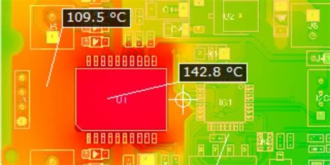
Thermal Stress: Excessive thermal stress can occur due to high operating temperatures, power surges, or during the soldering process. The differing thermal expansion coefficients of the materials used in the PCB can lead to stress buildup, resulting in delamination.
-
Mechanical Stress: Physical stress on the PCB, such as bending, twisting, or impact, can cause the layers to separate, especially if the adhesive bond is already weak.
-
Chemical Contamination: Exposure to certain chemicals, such as solvents or cleaning agents, can degrade the adhesive bond between the layers, making the PCB more prone to delamination.
Effects of PCB Delamination
PCB delamination can have severe consequences on the functionality and reliability of electronic devices:
-
Electrical Failure: Delamination can cause the conductive layers to separate, leading to open circuits or short circuits. This can result in the malfunction or complete failure of the electronic device.
-
Reduced Insulation: The separation of layers can compromise the insulation between the conductive paths, increasing the risk of electrical leakage or cross-talk between signals.
-
Decreased Mechanical Strength: Delamination weakens the overall mechanical structure of the PCB, making it more susceptible to physical damage or breakage.
-
Accelerated Aging: Delaminated regions can trap moisture and contaminants, accelerating the aging and deterioration of the PCB materials.
-
Intermittent Faults: Delamination can cause intermittent faults that are difficult to diagnose and repair, leading to increased maintenance costs and downtime.
Preventing PCB Delamination
To minimize the risk of PCB delamination, several preventive measures can be implemented during the design, manufacturing, and handling stages:
Design Considerations
-
Material Selection: Choose PCB materials with good thermal stability, low moisture absorption, and compatible thermal expansion coefficients to reduce the likelihood of delamination.
-
Proper Layer Stacking: Optimize the layer stacking arrangement to minimize thermal stress and ensure adequate adhesion between layers.
-
Controlled Impedance: Design controlled impedance traces to maintain consistent electrical characteristics and reduce the risk of signal integrity issues caused by delamination.
-
Stress Relief Features: Incorporate stress relief features, such as slots or cutouts, to alleviate mechanical stress concentrations that can lead to delamination.
Manufacturing Process Control
-
Lamination Parameter Optimization: Ensure that the lamination process parameters, such as temperature, pressure, and duration, are optimized for the specific PCB materials and thickness.
-
Moisture Control: Implement strict moisture control measures during the manufacturing process, including proper storage and handling of PCB materials, and the use of moisture barrier bags for transportation and storage.
-
Cleanliness and Contamination Prevention: Maintain a clean manufacturing environment to prevent chemical contamination that can degrade the adhesive bond between layers.
-
Quality Inspection: Conduct thorough visual and automated optical inspections (AOI) to detect any signs of delamination or other manufacturing defects.
Handling and Assembly Precautions
-
Moisture Sensitivity Level (MSL) Management: Follow the appropriate MSL handling guidelines, including baking and moisture-sensitive packaging, to prevent moisture absorption during storage and assembly.
-
Proper Soldering Techniques: Use appropriate soldering techniques, such as controlled heating and cooling rates, to minimize thermal stress on the PCB during assembly.
-
Mechanical Handling: Handle PCBs with care to avoid excessive bending, twisting, or impact that can cause delamination.
-
Environmental Control: Store and operate PCBs in a controlled environment with appropriate temperature and humidity levels to minimize the risk of moisture-related delamination.

Detecting and Addressing PCB Delamination
Despite preventive measures, PCB delamination can still occur. Early detection and appropriate actions are crucial to minimize the impact on the overall system.
Detection Methods
-
Visual Inspection: Regularly inspect PCBs for visible signs of delamination, such as blistering, swelling, or separation of layers.
-
Automated Optical Inspection (AOI): Use AOI systems to detect delamination during the manufacturing process or incoming quality control.
-
X-ray Imaging: Employ X-ray imaging techniques to detect internal delamination that may not be visible on the surface.
-
Acoustic Microscopy: Utilize acoustic microscopy to detect delamination by analyzing the reflection and transmission of high-frequency sound waves through the PCB.
Corrective Actions
-
Rework and Repair: If delamination is detected early and is limited to a small area, localized rework and repair techniques can be employed to address the issue.
-
Conformal Coating: Apply a conformal coating to the PCB to provide additional protection against moisture and mechanical stress, which can help prevent further delamination.
-
Redesign and Re-manufacture: In cases of severe or widespread delamination, it may be necessary to redesign the PCB and re-manufacture it with improved materials, processes, and design considerations.
-
Failure Analysis: Conduct a thorough failure analysis to identify the root cause of delamination and implement corrective actions to prevent recurrence in future production.

Conclusion
PCB delamination is a critical defect that can have severe consequences on the reliability and functionality of electronic devices. By understanding the causes, effects, and prevention methods of PCB delamination, designers, manufacturers, and assemblers can take proactive steps to minimize the occurrence of this circuit board blistering defect.
Implementing robust design practices, strict process controls, and proper handling procedures can significantly reduce the risk of PCB delamination. Early detection and appropriate corrective actions are essential to mitigate the impact of delamination on the overall system performance and reliability.
By addressing PCB delamination through a comprehensive approach, the electronics industry can enhance the quality, durability, and reliability of their products, ultimately leading to improved customer satisfaction and reduced costs associated with failures and repairs.

Frequently Asked Questions (FAQ)
-
What is the main cause of PCB delamination?
The main cause of PCB delamination is the failure of the adhesive bond between the layers of the circuit board. This can be due to various factors, such as improper lamination process, moisture absorption, thermal stress, mechanical stress, or chemical contamination. -
How does moisture absorption contribute to PCB delamination?
PCBs can absorb moisture from the environment, especially during the manufacturing process or in humid conditions. When the board is subjected to high temperatures, such as during soldering or operation, the absorbed moisture can vaporize and cause delamination by exerting pressure between the layers. -
What are the consequences of PCB delamination?
PCB delamination can lead to electrical failures, such as open circuits or short circuits, due to the separation of conductive layers. It can also reduce insulation, decrease mechanical strength, accelerate aging, and cause intermittent faults in the electronic device. -
How can PCB delamination be prevented during the design phase?
During the design phase, PCB delamination can be prevented by selecting materials with good thermal stability and low moisture absorption, optimizing the layer stacking arrangement, designing controlled impedance traces, and incorporating stress relief features. -
What are some methods for detecting PCB delamination?
PCB delamination can be detected through visual inspection, automated optical inspection (AOI), X-ray imaging, and acoustic microscopy. These methods help identify delamination at various stages, from manufacturing to incoming quality control and failure analysis.
| Cause | Effect |
|---|---|
| Improper Lamination Process | Weak bonds between layers, susceptible to delamination |
| Moisture Absorption | Vaporization and pressure buildup during high temperatures |
| Thermal Stress | Stress buildup due to differing thermal expansion coefficients |
| Mechanical Stress | Separation of layers due to bending, twisting, or impact |
| Chemical Contamination | Degradation of the adhesive bond between layers |
| Prevention Method | Description |
|---|---|
| Material Selection | Choose materials with good thermal stability and low moisture absorption |
| Proper Layer Stacking | Optimize layer arrangement to minimize thermal stress and ensure adhesion |
| Controlled Impedance | Design controlled impedance traces to maintain consistent electrical characteristics |
| Stress Relief Features | Incorporate features to alleviate mechanical stress concentrations |
| Lamination Parameter Optimization | Optimize lamination process parameters for specific PCB materials and thickness |
| Moisture Control | Implement strict moisture control measures during manufacturing and storage |
| Cleanliness and Contamination Prevention | Maintain a clean manufacturing environment to prevent chemical contamination |
| Quality Inspection | Conduct visual and automated optical inspections to detect delamination |


Leave a Reply