Introduction to PCB Art
PCB art is a unique form of artistic expression that combines the functionality of printed circuit boards (PCBs) with striking visual designs. By incorporating artistic elements into the layout and design of PCBs, engineers and artists can create visually stunning boards that not only serve their electronic purpose but also stand out as works of art.
In this comprehensive guide, we will explore the world of PCB art, discussing the techniques, tools, and considerations involved in creating a striking and visually appealing PCB design. Whether you are an experienced PCB designer looking to add an artistic flair to your projects or an artist interested in exploring the intersection of technology and art, this article will provide you with valuable insights and inspiration.
The Basics of PCB Design
Before delving into the artistic aspects of PCB design, it is essential to understand the basics of PCB layout and functionality. A printed circuit board is a flat board made of insulating material, such as fiberglass or plastic, with conductive copper traces etched onto its surface. These traces connect various electronic components, such as resistors, capacitors, and integrated circuits, to form a complete electronic circuit.
Key Components of a PCB
- Substrate: The insulating material that forms the base of the PCB.
- Copper Layers: The conductive layers that carry electrical signals between components.
- Solder Mask: A protective coating that covers the copper traces, preventing short circuits and oxidation.
- Silkscreen: A layer of text and symbols printed on the PCB for identification and assembly purposes.
- Vias: Conductive holes that allow electrical connections between different layers of the PCB.
Understanding these basic components and their roles in PCB design will help you create visually appealing boards that maintain their functionality.

Planning Your PCB Art Design
Before starting your PCB art project, it is crucial to plan your design carefully. Consider the following factors:
1. Purpose and Functionality
While creating a visually stunning PCB is the primary goal of PCB art, it is essential to ensure that the board still serves its intended electronic purpose. Consider the circuit requirements, component placement, and signal integrity when planning your design.
2. Artistic Vision
Determine the overall aesthetic you want to achieve with your PCB art. Consider the theme, color scheme, and visual elements you want to incorporate into your design. Sketch out your ideas and create a rough layout to guide your design process.
3. Manufacturing Constraints
Keep in mind the manufacturing constraints and limitations when planning your PCB art. Factors such as minimum trace width, clearance between components, and available board sizes will impact your design choices.

Techniques for Creating PCB Art
There are several techniques you can employ to create striking and visually appealing PCB art designs:
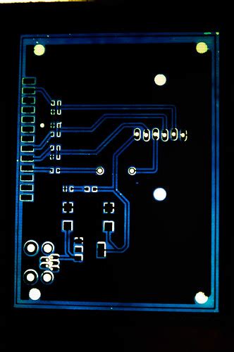
1. Trace Routing
One of the most fundamental techniques in PCB art is creative trace routing. By carefully designing the paths of the copper traces, you can create intricate patterns, shapes, and even images on the PCB surface. Consider the following tips when routing traces for artistic effect:
- Use curved and organic shapes to add visual interest
- Incorporate symmetry and repetition to create patterns
- Vary trace widths to emphasize certain elements
- Use hatching or cross-hatching techniques to add texture
2. Silkscreen Design
The silkscreen layer of a PCB offers another opportunity for artistic expression. By carefully designing the text, symbols, and graphics printed on the silkscreen, you can enhance the overall visual impact of your PCB art. Consider the following ideas:
- Use custom fonts or handwritten text for a unique look
- Incorporate logos, icons, or illustrations related to your project theme
- Create borders, frames, or decorative elements using the silkscreen
- Use the silkscreen to label components or provide assembly instructions
3. Component Selection and Placement
The selection and placement of electronic components can also contribute to the artistic appeal of your PCB. Consider the following techniques:
- Choose components with unique shapes or colors to add visual interest
- Arrange components in patterns or geometric shapes
- Use component placement to emphasize certain areas of your design
- Incorporate non-functional components, such as LEDs or decorative elements, for aesthetic purposes
4. Solder Mask and Finish Options
The choice of solder mask color and surface finish can significantly impact the overall look of your PCB art. Experiment with different solder mask colors, such as green, blue, red, or even transparent, to complement your design. Additionally, consider using special surface finishes, such as matte, glossy, or metallic, to add depth and texture to your board.

Tools and Software for PCB Art Design
To create PCB art, you will need access to PCB design software and various tools. Some popular software options for PCB art include:
- KiCad: A free, open-source PCB design software with a wide range of features and a large user community.
- Eagle: A widely used PCB design software that offers a free version for non-commercial use.
- Altium Designer: A professional-grade PCB design software with advanced features and a steep learning curve.
- Autodesk Fusion 360: A powerful 3D modeling and PCB design software that offers a free version for personal use.
In addition to software, you may also need access to a laser printer, UV exposure unit, and etching equipment if you plan to manufacture your PCB art in-house.
Showcasing Your PCB Art
Once you have created your PCB art, it is time to showcase your work. Consider the following ideas for displaying and sharing your PCB art:
- Framing: Mount your PCB art in a custom frame to display it as a piece of artwork.
- Photography: Take high-quality photographs of your PCB art to share online or in portfolios.
- Social Media: Share your PCB art on social media platforms, such as Instagram or Twitter, using relevant hashtags to reach a wider audience.
- Exhibitions: Participate in art exhibitions or maker faires to showcase your PCB art alongside other creative works.
- Collaboration: Collaborate with other artists, designers, or engineers to create unique PCB art projects.
Frequently Asked Questions (FAQ)
-
Q: Do I need to have prior experience in PCB design to create PCB art?
A: While prior experience in PCB design can be helpful, it is not strictly necessary. Many PCB art projects can be created using basic PCB design principles and a creative approach. However, it is essential to understand the fundamentals of PCB design to ensure that your artwork is functional and manufacturable. -
Q: Can I use any PCB design software to create PCB art?
A: Most PCB design software packages can be used to create PCB art, as they provide the necessary tools for designing and routing traces, placing components, and creating silkscreen designs. Some software may offer additional features or libraries that can be particularly useful for artistic purposes. -
Q: How can I ensure that my PCB art is manufacturable?
A: To ensure that your PCB art is manufacturable, it is essential to adhere to the design guidelines and constraints provided by your chosen PCB manufacturer. This includes minimum trace widths, clearances, and drill sizes. It is also a good idea to communicate with your manufacturer and provide them with detailed design files and specifications to avoid any issues during production. -
Q: Are there any limitations to the artistic elements I can incorporate into my PCB art?
A: While PCB art offers a wide range of creative possibilities, there are some limitations to keep in mind. The physical constraints of PCB manufacturing, such as minimum trace widths and clearances, may limit the level of detail and intricacy you can achieve in your designs. Additionally, the choice of components and their placement may be dictated by the functional requirements of your circuit. -
Q: Can I sell my PCB art designs or use them for commercial purposes?
A: Yes, you can sell your PCB art designs or use them for commercial purposes, subject to any applicable licenses or agreements. If you are using third-party components, libraries, or design elements in your artwork, be sure to review and comply with their respective licenses and terms of use. When selling your PCB art, it is important to clearly communicate the intended use and any limitations to your customers.
Conclusion
PCB art is a fascinating intersection of technology and artistic expression, allowing designers and artists to create visually stunning and functional electronic boards. By understanding the basics of PCB design, planning your artistic vision, and employing various techniques such as creative trace routing, silkscreen design, and component selection, you can create striking PCB art that stands out from conventional circuit boards.
Remember to consider the manufacturing constraints and communicate with your chosen PCB manufacturer to ensure that your designs are feasible and can be produced effectively. With the right tools, software, and creative approach, the possibilities for PCB art are virtually endless.
We hope that this comprehensive guide has provided you with valuable insights and inspiration to embark on your own PCB art journey. Whether you are an experienced PCB designer looking to add an artistic flair to your projects or an artist exploring the world of electronics, PCB art offers a unique and rewarding medium for creative expression. So, grab your tools, fire up your design software, and let your imagination run wild as you create your own striking and visually stunning PCB art designs.
| Technique | Description | Tips |
|---|---|---|
| Trace Routing | Creating intricate patterns and shapes using copper traces | – Use curved and organic shapes – Incorporate symmetry and repetition – Vary trace widths – Use hatching or cross-hatching techniques |
| Silkscreen Design | Designing text, symbols, and graphics on the silkscreen layer | – Use custom fonts or handwritten text – Incorporate logos, icons, or illustrations – Create borders, frames, or decorative elements – Use silkscreen for labeling or assembly instructions |
| Component Selection and Placement | Choosing and arranging components for artistic effect | – Choose components with unique shapes or colors – Arrange components in patterns or geometric shapes – Use component placement to emphasize certain areas – Incorporate non-functional components for aesthetics |
| Solder Mask and Finish Options | Experimenting with different solder mask colors and surface finishes | – Choose solder mask colors to complement your design – Consider special surface finishes like matte, glossy, or metallic |


Leave a Reply