Introduction to Parasitic Capacitances
Parasitic capacitances are unwanted and unavoidable capacitances that occur between conductors in electronic circuits. These capacitances can have significant effects on the performance and behavior of the circuit, especially at high frequencies. Understanding parasitic capacitances is crucial for designing and analyzing electronic circuits, particularly in the fields of radio frequency (RF) and high-speed digital systems.
What is Capacitance?
Capacitance is the ability of a system to store electrical charge. It is a fundamental property of any two conductors separated by an insulator or dielectric material. The capacitance between two conductors is determined by the geometry of the conductors and the properties of the dielectric material between them.
The basic equation for capacitance is:
C = ε * A / d
Where:
– C is the capacitance in farads (F)
– ε is the permittivity of the dielectric material (F/m)
– A is the area of the conductors (m^2)
– d is the distance between the conductors (m)
Types of Parasitic Capacitances
Parasitic capacitances can occur in various forms within electronic circuits. The most common types of parasitic capacitances are:
-
Coupling Capacitance: This occurs between adjacent conductors or traces on a printed circuit board (PCB). The closer the conductors are to each other, the higher the coupling capacitance.
-
Fringing Capacitance: This occurs at the edges of conductors where the electric field lines bend outwards, creating additional capacitance.
-
Substrate Capacitance: In integrated circuits (ICs), parasitic capacitance can occur between the conductors and the substrate or bulk material on which the circuit is fabricated.
-
Package Capacitance: The packaging of electronic components, such as IC packages or discrete components, can introduce parasitic capacitances between the pins or leads.
Effects of Parasitic Capacitances on Circuit Performance
Signal Integrity Issues
Parasitic capacitances can have a significant impact on signal integrity in high-speed digital circuits. As the frequency of the signals increases, the effects of parasitic capacitances become more pronounced. Some of the signal integrity issues caused by parasitic capacitances include:
-
Signal Distortion: Parasitic capacitances can cause the shape of the signal to be distorted, leading to ringing, overshoot, or undershoot. This can result in false triggering or incorrect data interpretation.
-
Crosstalk: Coupling capacitance between adjacent signal lines can cause crosstalk, where the signal on one line interferes with the signal on another line. This can lead to data corruption or errors.
-
Propagation Delay: Parasitic capacitances can increase the propagation delay of signals, as the capacitances need to be charged and discharged during signal transitions. This can limit the maximum operating frequency of the circuit.
Frequency Response and Bandwidth Limitations
Parasitic capacitances can also affect the frequency response and bandwidth of electronic circuits. In analog circuits, such as amplifiers or filters, parasitic capacitances can create unwanted poles or zeros in the transfer function, altering the desired frequency response.
In RF circuits, parasitic capacitances can limit the bandwidth and cause frequency-dependent losses. The reactance of the parasitic capacitances decreases with increasing frequency, leading to increased signal attenuation and reduced quality factor (Q) of resonant circuits.

Techniques for Minimizing Parasitic Capacitances
PCB Layout Techniques
Proper PCB layout is essential for minimizing parasitic capacitances. Some techniques to reduce parasitic capacitances in PCB designs include:
-
Increasing Trace Spacing: Increasing the spacing between adjacent traces reduces the coupling capacitance between them. This can be achieved by using wider trace spacing or by adding ground traces between signal traces.
-
Minimizing Trace Lengths: Shorter traces have lower parasitic capacitances compared to longer traces. Minimizing trace lengths by placing components close together and using direct routing can help reduce parasitic capacitances.
-
Using Ground Planes: Incorporating ground planes in the PCB layout helps to shield the signal traces from each other, reducing coupling capacitance. The ground plane also provides a low-impedance return path for the signals, improving signal integrity.
-
Optimizing Layer Stackup: The layer stackup of the PCB can be optimized to reduce parasitic capacitances. By placing signal layers close to their respective ground or power planes, the loop area and resulting inductance can be minimized.
Component Selection and Placement
The selection and placement of components can also impact parasitic capacitances in the circuit. Some considerations include:
-
Choosing Low-Capacitance Components: When possible, select components with low parasitic capacitances, such as surface-mount devices (SMDs) with small package sizes or low-capacitance variants of components.
-
Minimizing Lead Lengths: Shorter component leads or pins have lower parasitic capacitances compared to longer ones. Using SMDs or components with shorter leads can help reduce parasitic capacitances.
-
Strategic Component Placement: Place components strategically to minimize the coupling capacitance between them. Avoid placing sensitive components near high-speed or high-frequency signals to reduce crosstalk.
Simulation and Modeling Techniques
Simulation and modeling techniques can be used to analyze and optimize circuits for parasitic capacitances. Some commonly used techniques include:
-
SPICE Simulation: SPICE (Simulation Program with Integrated Circuit Emphasis) is a widely used circuit simulation tool that can model parasitic capacitances. By including parasitic capacitances in the simulation model, designers can assess their impact on circuit performance and make necessary adjustments.
-
Electromagnetic (EM) Simulation: EM simulation tools, such as finite-element method (FEM) or method of moments (MoM), can provide detailed analysis of the electromagnetic fields and parasitic capacitances in complex structures like PCBs or ICs. These simulations help identify potential issues and optimize the design.
-
Equivalent Circuit Modeling: Parasitic capacitances can be modeled as lumped elements in an equivalent circuit model. By representing the parasitic capacitances as capacitors in the circuit schematic, designers can analyze their effects and make appropriate design changes.

Measuring and Characterizing Parasitic Capacitances
Measurement Techniques
Measuring parasitic capacitances is important for validating the design and ensuring the actual circuit performance matches the simulated or expected behavior. Some common measurement techniques for parasitic capacitances include:
-
Time-Domain Reflectometry (TDR): TDR is a technique that measures the reflections of a fast-rise-time pulse sent through the circuit. By analyzing the reflected waveform, the parasitic capacitances can be extracted.
-
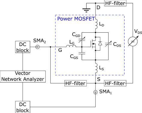
Vector Network Analyzer (VNA): A VNA measures the scattering parameters (S-parameters) of a circuit over a range of frequencies. By analyzing the S-parameters, the parasitic capacitances can be determined.
-
Impedance Analyzer: An impedance analyzer measures the complex impedance of a circuit over a range of frequencies. The parasitic capacitances can be extracted from the impedance data.
Characterization and Modeling
Once the parasitic capacitances are measured, they need to be characterized and modeled for use in simulations and design optimizations. Some important aspects of parasitic capacitance characterization and modeling include:
-
Extracting Capacitance Values: The measured data is analyzed to extract the capacitance values associated with different parts of the circuit. This can be done using equivalent circuit models or by fitting the data to mathematical expressions.
-
Creating Behavioral Models: Behavioral models, such as SPICE subcircuits or mathematical equations, are created to represent the parasitic capacitances in simulations. These models capture the essential behavior of the parasitic capacitances without the need for detailed physical modeling.
-
Validating Models: The developed models are validated against the measured data to ensure their accuracy and reliability. This involves comparing the simulated results with the measured data and making necessary adjustments to the models.

Case Studies and Examples
Example 1: High-Speed Digital Interface
Consider a high-speed digital interface, such as a DDR (Double Data Rate) memory interface. Parasitic capacitances can have a significant impact on the signal integrity and timing of the data lines.
| Parameter | Value |
|---|---|
| Data Rate | 3200 MT/s |
| Trace Length | 5 cm |
| Trace Width | 0.2 mm |
| Trace Spacing | 0.2 mm |
| Dielectric Constant (εr) | 4.0 |
In this example, the coupling capacitance between adjacent data lines can cause crosstalk and signal distortion. By using techniques like increasing trace spacing, minimizing trace lengths, and using ground shields, the parasitic capacitances can be reduced, improving the signal integrity and allowing for reliable data transmission at high speeds.
Example 2: RF Amplifier
Consider an RF amplifier operating at a frequency of 2.4 GHz. Parasitic capacitances in the amplifier circuit can affect the frequency response and gain of the amplifier.
| Parameter | Value |
|---|---|
| Operating Frequency | 2.4 GHz |
| Transistor Capacitance | 0.5 pF |
| PCB Trace Capacitance | 0.2 pF |
| Package Capacitance | 0.3 pF |
In this example, the parasitic capacitances of the transistor, PCB traces, and package can create unwanted resonances or limit the bandwidth of the amplifier. By carefully selecting low-capacitance components, optimizing the PCB layout, and using EM simulation tools, the impact of parasitic capacitances can be minimized, resulting in improved amplifier performance.
Frequently Asked Questions (FAQ)
-
What are parasitic capacitances and why are they important?
Parasitic capacitances are unwanted and unavoidable capacitances that occur between conductors in electronic circuits. They are important because they can have significant effects on the performance and behavior of the circuit, especially at high frequencies, leading to signal integrity issues, frequency response degradation, and bandwidth limitations. -
How do parasitic capacitances affect signal integrity in high-speed digital circuits?
Parasitic capacitances can cause signal distortion, crosstalk, and increased propagation delay in high-speed digital circuits. Signal distortion can lead to false triggering or incorrect data interpretation, while crosstalk can cause interference between adjacent signal lines, resulting in data corruption or errors. Increased propagation delay due to parasitic capacitances can limit the maximum operating frequency of the circuit. -
What are some PCB layout techniques to minimize parasitic capacitances?
Some PCB layout techniques to minimize parasitic capacitances include increasing trace spacing, minimizing trace lengths, using ground planes, and optimizing layer stackup. Increasing trace spacing reduces coupling capacitance between adjacent traces, while minimizing trace lengths reduces the overall parasitic capacitance. Ground planes help shield signal traces from each other and provide a low-impedance return path. Optimizing layer stackup by placing signal layers close to their respective ground or power planes helps minimize loop area and inductance. -
How can simulation and modeling techniques help in analyzing and optimizing circuits for parasitic capacitances?
Simulation and modeling techniques, such as SPICE simulation, electromagnetic (EM) simulation, and equivalent circuit modeling, can help analyze and optimize circuits for parasitic capacitances. SPICE simulation allows designers to include parasitic capacitances in the simulation model and assess their impact on circuit performance. EM simulation tools provide detailed analysis of electromagnetic fields and parasitic capacitances in complex structures like PCBs or ICs. Equivalent circuit modeling represents parasitic capacitances as lumped elements in the circuit schematic, enabling designers to analyze their effects and make appropriate design changes. -
What are some common measurement techniques for characterizing parasitic capacitances?
Common measurement techniques for characterizing parasitic capacitances include time-domain reflectometry (TDR), vector network analyzer (VNA), and impedance analyzer. TDR measures the reflections of a fast-rise-time pulse sent through the circuit, allowing the extraction of parasitic capacitances from the reflected waveform. VNA measures the scattering parameters (S-parameters) of a circuit over a range of frequencies, enabling the determination of parasitic capacitances. Impedance analyzer measures the complex impedance of a circuit over a range of frequencies, from which parasitic capacitances can be extracted.
Conclusion
Parasitic capacitances are an inevitable reality in electronic circuits, and their effects become more pronounced as frequencies increase and circuit dimensions shrink. Understanding the sources, effects, and mitigation techniques for parasitic capacitances is crucial for designing high-performance electronic systems.
By employing proper PCB layout techniques, selecting appropriate components, and utilizing simulation and modeling tools, designers can minimize the impact of parasitic capacitances on circuit performance. Measurement and characterization techniques enable the validation of designs and the development of accurate models for simulation and optimization.
As electronic systems continue to push the boundaries of speed and complexity, the management of parasitic capacitances will remain a critical aspect of circuit design. By staying informed about the latest techniques and tools for dealing with parasitic capacitances, engineers can effectively navigate the challenges and design circuits that deliver optimal performance in the presence of these unwanted and unavoidable charges.


Leave a Reply