Introduction to PCB Design and PADS Software
Printed Circuit Board (PCB) design is a crucial aspect of electronic product development. It involves the layout and routing of electronic components on a board to create a functional circuit. PADS is a powerful PCB design software that offers a comprehensive set of tools for designing, simulating, and documenting PCBs. In this tutorial, we will guide you through the process of designing a PCB using PADS software.
What is PCB Design?
PCB design is the process of creating a layout for electronic components on a printed circuit board. It involves the placement of components, routing of traces, and the creation of a final design that can be manufactured. PCB design requires knowledge of electronic components, circuit design, and PCB manufacturing processes.
Why Use PADS for PCB Design?
PADS is a popular PCB design software that offers a range of features and tools for designing high-quality PCBs. Some of the key benefits of using PADS include:
- Intuitive user interface
- Powerful design and simulation tools
- Comprehensive library of electronic components
- Seamless integration with other design tools
- Extensive documentation and support resources
Getting Started with PADS
System Requirements
Before you start using PADS, ensure that your computer meets the following system requirements:
| Operating System | Processor | RAM | Hard Disk Space |
|---|---|---|---|
| Windows 10/11 | Intel Core i5 or higher | 8 GB or more | 20 GB or more |
Installing PADS
To install PADS, follow these steps:
- Download the PADS installer from the official website.
- Run the installer and follow the on-screen instructions.
- Activate your license using the provided activation code.
- Launch PADS and start designing your PCB.

PADS User Interface
Main Window
The main window of PADS consists of several key areas:
- Menu Bar: Contains various menu options for accessing different tools and features.
- Toolbar: Provides quick access to commonly used tools and commands.
- Design Area: The main area where you create and edit your PCB design.
- Layers Panel: Allows you to manage different layers of your PCB design.
- Properties Panel: Displays properties of selected objects in your design.
Customizing the User Interface
PADS allows you to customize the user interface to suit your preferences. Some of the customization options include:
- Rearranging panels and toolbars
- Changing color schemes and themes
- Creating custom keyboard shortcuts
- Saving and loading custom workspace layouts

Creating a New PCB Design
Setting Up the Design
To create a new PCB design in PADS, follow these steps:
- Click on “File” > “New” > “PCB Design”.
- Specify the design name, location, and other project settings.
- Choose the board size, layer stack-up, and design rules.
- Click “OK” to create the new design.
Importing Schematic
If you have a schematic design created in another tool, you can import it into PADS using the following steps:
- Click on “File” > “Import” > “Schematic”.
- Select the schematic file and click “Open”.
- Map the schematic components to PADS library components.
- Review and approve the imported design.

Placing Components
Component Libraries
PADS comes with a comprehensive library of electronic components that you can use in your designs. To access the component libraries:
- Click on “Tools” > “Component Library Manager”.
- Browse through the available libraries and select the components you need.
- Drag and drop the selected components onto your design area.
Manual Placement
To manually place components on your PCB:
- Select the component from the library panel.
- Click on the desired location on the PCB to place the component.
- Rotate and adjust the component as needed using the tools in the toolbar.
Automatic Placement
PADS also offers automatic component placement tools to save time and effort:
- Click on “Tools” > “Auto Place”.
- Specify the placement parameters such as component spacing and orientation.
- Review and adjust the automatically placed components if needed.
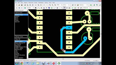
Routing Traces
Manual Routing
To manually route traces between components:
- Select the “Route” tool from the toolbar.
- Click on the starting pad and then click on the ending pad to create a trace.
- Adjust the trace width and layer as needed using the properties panel.
Automatic Routing
PADS offers automatic routing tools to route traces between components quickly:
- Click on “Tools” > “Auto Route”.
- Specify the routing parameters such as via size and trace width.
- Review and adjust the automatically routed traces if needed.
Design Rule Check (DRC)
To ensure that your PCB design meets the manufacturing requirements, PADS provides a Design Rule Check (DRC) tool:
- Click on “Tools” > “Design Rule Check”.
- Specify the design rules such as minimum trace width and clearance.
- Run the DRC and review any violations reported.
- Fix the violations and re-run the DRC until the design passes all checks.
Generating Output Files
Gerber Files
To generate Gerber files for PCB manufacturing:
- Click on “File” > “Export” > “Gerber”.
- Specify the output directory and file format settings.
- Select the layers to be exported.
- Click “Export” to generate the Gerber files.
Drill Files
To generate drill files for PCB manufacturing:
- Click on “File” > “Export” > “Drill”.
- Specify the output directory and file format settings.
- Select the drill sizes and layers to be exported.
- Click “Export” to generate the drill files.
Bill of Materials (BOM)
To generate a Bill of Materials (BOM) for your PCB:
- Click on “File” > “Export” > “BOM”.
- Specify the output directory and file format settings.
- Select the fields to be included in the BOM.
- Click “Export” to generate the BOM file.
Frequently Asked Questions (FAQ)
1. What is the difference between PCB design and schematic design?
Schematic design involves creating a diagram of the electronic circuit showing the components and their connections. PCB design, on the other hand, involves creating a physical layout of the circuit on a printed circuit board, including the placement of components and routing of traces.
2. Can I use PADS for both schematic and PCB design?
Yes, PADS offers an integrated environment for both schematic and PCB design. You can create your schematic in PADS and then easily transfer it to the PCB design environment for layout and routing.
3. How do I know which components to use in my PCB design?
The choice of components depends on the specific requirements of your circuit, such as voltage, current, and functionality. You can consult datasheets, application notes, and reference designs to select the appropriate components for your design.
4. What are the different layers in a PCB?
A typical PCB consists of several layers, including:
- Top Layer: Contains components and traces on the top side of the board.
- Bottom Layer: Contains components and traces on the bottom side of the board.
- Inner Layers: Used for additional routing and power/ground planes.
- Solder Mask: Insulating layer that covers the copper traces, leaving only the pads exposed.
- Silkscreen: Text and graphics printed on the PCB for identification and assembly.
5. How do I ensure that my PCB design is manufacturable?
To ensure that your PCB design is manufacturable, follow these guidelines:
- Adhere to the design rules and constraints specified by the PCB manufacturer.
- Use standard component sizes and packages.
- Provide adequate spacing between components and traces.
- Minimize the number of layers and vias to reduce manufacturing cost and complexity.
- Generate accurate and complete manufacturing files, including Gerber and drill files.
Conclusion
PCB design is a critical aspect of electronic product development, and PADS software provides a powerful and intuitive environment for designing high-quality PCBs. By following this step-by-step tutorial, you should now have a good understanding of the PCB design process using PADS, from setting up the design and placing components to routing traces and generating manufacturing files. With practice and experience, you can create complex and reliable PCB designs using PADS.


Leave a Reply