
Introduction
Printed circuit boards (PCBs) are essential components in nearly all modern electronic devices. As electronics become smaller and more complex, there is a growing need for PCBs that are compact and can flex to fit within tight spaces. This is where multilayer flex PCBs come in.
Multilayer flex PCBs provide several advantages over traditional rigid PCBs:
Flexibility
As the name implies, multilayer flex PCBs can bend and flex. This allows them to be installed in spaces where a rigid board simply wouldn’t fit. The flexibility also reduces the risk of mechanical stress and failure.
High Component Density
By using flexible substrate materials, multilayer flex PCBs can have more layers than rigid boards. This means more space for routing traces and mounting components in a compact area. Dense component mounting is critical for smaller electronics like smartphones.
Reliability
The flexibility of the boards accommodates vibration, shock, and temperature changes that would damage a rigid board. This makes multilayer flex PCBs well-suited for medical, aerospace, automotive and other demanding applications.
Light Weight
Multilayer flex PCBs use thin, lightweight material layers. This reduces the total weight of the finished product. Weight is an important consideration for mobile and wearable devices.
In this article, we’ll dive deeper into multilayer flex PCB technology and discuss its design, manufacturing, and applications.
Multilayer Flex PCB Construction
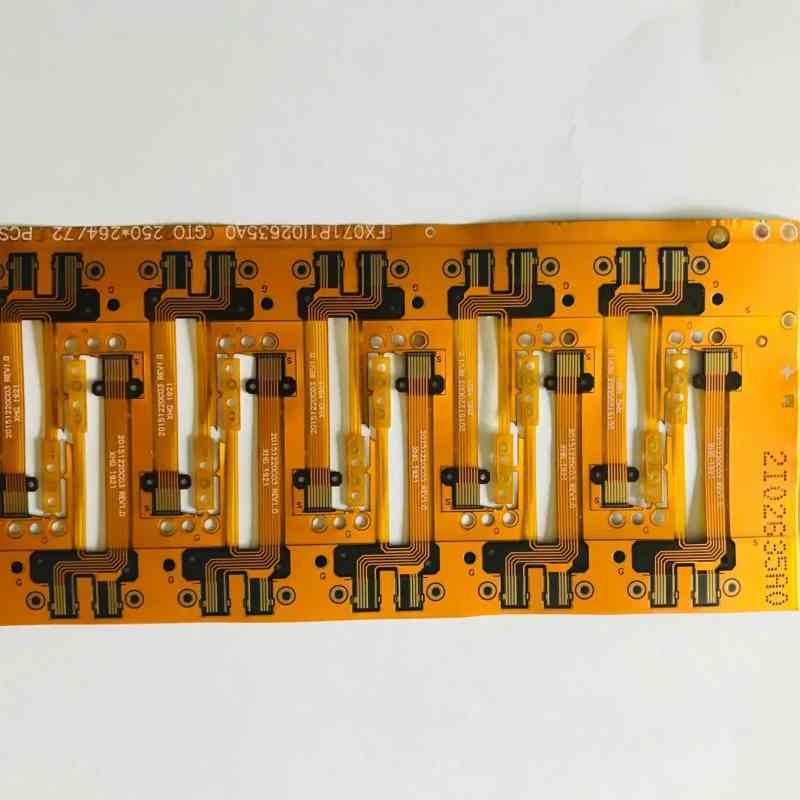
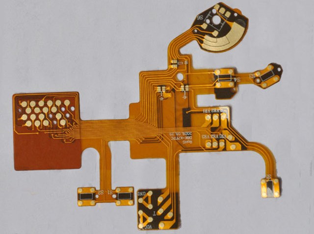
A multilayer flex PCB consists of flexible substrate layers bonded together with adhesive. Popular substrate materials include polyimide (Kapton), polyester (PET), and PEN. Metal traces are patterned on each layer to form the circuits. Vias provide electrical connections between layers. Components are mounted on the surface.
Here are some key elements of a multilayer flex PCB stackup:
Flexible Substrate
The thin, flexible plastic film that forms the framework of the PCB. Polyimide is most common due to its excellent thermal and chemical resistance.
Metal Foil
Usually copper foil that is laminated onto the substrate. Thin foils from 1-3 oz (35-105 μm) are typical for flexibility.
Adhesive
Bonds the substrate layers together. Flexible acrylic, epoxy, or polyimide adhesives are commonly used.
Coverlay
A protective coating applied to the top and bottom outer surfaces. Covers and insulates the traces.
Solder Mask
An epoxy-based coating that protects the copper traces from oxidation and prevents solder bridges.
Stiffeners
Optional rigid sections for mounting components or connectors. Allow flexing in select areas only.
The cross-section above shows a typical 6-layer flex PCB stackup. The thin, flexible substrate and adhesive layers allow the board to bend and fold. Familiar PCB features like traces, vias, pads, and solder mask are also present.
Component mounting options include:
- Surface mount – Chips and packages soldered directly to pads on the outer layers
- Through hole – Leaded components inserted into plated through holes
- Embedded – Components placed between layers and encapsulated by the PCB
Design Guidelines
Designing a multilayer flex PCB requires following specialized design rules to ensure the board can physically bend and fold without damage. Here are some key guidelines:
Trace Width/Spacing
Use larger trace widths and spacing than on rigid boards to account for flexing. Common widths are 0.05-0.2 mm.
Pad Size
Pads should be enlarged to at least 0.3 mm minimum to withstand flex stress.
Hole Size
Plated through holes must have adequate annular rings to avoid cracking. 0.2 mm minimum annular ring width is recommended.
Bend Radius
Avoid sharp bends. Use minimum bend radii of 2-3X the board thickness for 90° bends. Gradual curves are preferred.
Stiffeners
Strategically place unetched areas of copper or additional material to create stiff sections. Allow flexing only in designated fold areas.
Adhesives
Choose flexible, high adhesion adhesives suitable for dynamic flexing applications. Acrylic or polyimide adhesives have good performance.
Component Placement
Position components in neutral bend areas away from fold lines and edges. Use flexible solder joints.
By following these guidelines, the PCB layout can be optimized for both flexibility and reliability under bending and other mechanical stresses.
Example 4-Layer Flex PCB Stackup
Here is an example 4-layer flex PCB stackup designed for optimal flexibility:
| Layer | Thickness | Material | Notes |
|---|---|---|---|
| 1 | 25 μm | Polyimide substrate | Thin, flexible layer |
| 2 | 18 μm | Copper traces | 1 oz. foil, etched traces |
| 3 | 25 μm | Adhesive | Flexible polyimide adhesive |
| 4 | 25 μm | Polyimide substrate | Thin, flexible layer |
| 5 | 18 μm | Copper ground plane | Unetched layer for shielding |
| 6 | 25 μm | Adhesive | Flexible acrylic adhesive |
| 7 | 25 μm | Polyimide substrate | Thin, flexible layer |
| 8 | 18 μm | Copper traces | 1 oz. foil, etched traces |
| 9 | 25 μm | Solder mask | Green epoxy solder mask |
| 10 | N/A | Legend | Surface mount pads and markings |
Total Thickness = 0.19 mm (7.5 mils)
This stackup uses four alternating layers of thin polyimide substrate bonded with flexible acrylic and polyimide adhesives. The thin 1 oz. copper and wide trace spacing provide flexibility. The sequence ensures no stiff copper layers are adjacent. The result is a PCB that can bend and fold in multiple directions.
Manufacturing Process
Multilayer flex PCB fabrication involves specialized processes to create thin, flexible circuit layers and bond them together. Here is a simplified overview of the manufacturing process:
1. Substrate Preparation
The flexible plastic substrate material such as polyimide is cut into sheets. Prepreg adhesive layers are also prepared.
2. Foil Lamination
Thin copper foil is laminated onto the substrate using heat and pressure to form a bond.
3. Photolithography
The foil is coated with photoresist and then exposed to UV light through a mask to transfer the circuit pattern.
4. Etching
The unexposed areas of copper are etched away, leaving the desired circuit traces protected by resist.
5. Layer Stackup
The etched flexible layers are precisely aligned and bonded together using adhesive between each layer.
6. Component Assembly
Components are soldered onto the pads and traces on the outer circuit layers.
7. Testing
The finished boards are electrically tested to verify the circuits are functioning correctly.
8. Final Protection
Additional coatings like solder mask and coverlay are applied to protect the flex PCB for its operating environment.
The specialized materials, handling, and stacking require advanced manufacturing equipment and processes tuned for flex PCB production. Complex alignment and bonding of many thin layers with high yield is challenging.
Key Applications
The unique properties of multilayer flex PCBs make them well-suited for many advanced electronics applications:
Consumer Electronics
Mobile phones, wearables, display devices, and other compact consumer electronics take advantage of the small size, light weight, and resilience of flex circuits. The flexibility allows conforming to product shapes and mechanics. High layer counts accommodate complex circuit needs in limited space.
Medical
Implantable medical devices such as hearing aids and body sensors require boards that are extremely light and flexible yet reliable for long term use. Multilayer flex PCBs meet the demands with biocompatible, robust construction ideal for medical uses.
Automotive
As automotive electronics expand, flex PCBs support mounting PCBs into tight spaces and onto interior surfaces. Flex-to-rigid boards combine flexible segments for connections with rigid segments for component mounts. The vibration resistance prevents cracking and failure.
Aerospace/Military
Avionics, radars, guidance systems, and other aerospace electronics operate in demanding environments. Multilayer flex PCBs withstand vibration, shock, and wide temperature swings for reliable performance under extreme conditions.
Wearable Electronics
For smartwatches, fitness trackers, VR headsets, and emerging body-borne electronics, multilayer flex PCBs provide the ideal combination of small size, light weight, and ruggedness to mount directly on clothing and the human body comfortably.
As electronics evolve to be smaller, lighter, and more powerful, multilayer flex PCB technology will continue growing to meet those demands where rigid boards fall short.
FQA
What are the key benefits of multilayer flex PCBs?
The main benefits are flexibility to fit tight spaces, ability to have high layer counts for complex circuits, lightweight/low mass design, and resilience against vibration, shock, and flexing. This makes them well suited for space-constrained and high reliability applications.
How many layers can flex PCBs support?
Advanced flex PCBs can have 12, 20, even 30+ layers. As a comparison, typical rigid boards max out around 16 layers. The flexible construction allows far higher layer counts in a compact stackup.
Can components be mounted on both sides of a flex PCB?
Yes, the outer layers of a multilayer flex PCB typically have exposed traces/pads for mounting surface mount components. Through-hole components can also be used. Careful design is needed around the flex areas.
What are some key rules for routing flex PCBs?
Use conservative trace spacing/widths, avoid 90° angles on traces, distribute traces evenly, use gradual bends, avoid component placement on bends. These help avoid stress points when flexed.
How is impedance controlled on flex PCBs?
Thicker flex layers, spacing to planes, and trace width adjustments help control impedance on flex PCBs. It is more challenging than with rigid boards due to the thinner dielectrics. Matching lengths and widths is critical.


Leave a Reply