Introduction to Substrate-Bonded PCBs
A printed circuit board (PCB) mechanically supports and electrically connects electronic components using conductive tracks, pads and other features etched from one or more sheet layers of copper that are laminated onto and/or between sheet layers of a non-conductive substrate. Substrate-bonded PCBs take this a step further by utilizing an additive process to bond the copper layer directly to the substrate material.
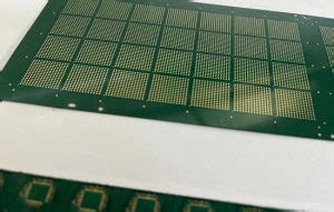
The modified Semi-Additive Process (mSAP) is an advanced PCB manufacturing method that enables finer circuit features and higher interconnect density compared to traditional subtractive etching processes. By depositing thin copper layers onto the dielectric substrate and then selectively removing the unwanted copper, mSAP can produce copper traces and spaces down to 30µm wide. This allows more compact designs, improved signal integrity, and greater reliability.
Advantages of mSAP Substrate-Bonded PCBs
Compared to standard subtractively-etched PCBs, mSAP substrate-bonded PCBs offer several key benefits:
- Finer pitch and higher wiring density (traces/spaces down to 30/30µm)
- Thinner copper weight for reduced conductor losses at high frequencies
- Ultra-thin substrates down to 25µm for increased flexibility
- Improved adhesion between copper and substrate for greater reliability
- Elimination of glass fibers protruding from drilled holes
- Capability for stacked microvias, blind/buried vias, and via-in-pad
- Smooth copper surface for better signal integrity and underfilling
mSAP PCB Manufacturing Process
The mSAP technique for fabricating substrate-bonded PCBs involves depositing a thin layer of copper directly onto the dielectric substrate material, and then selectively etching away the unwanted copper to form the desired circuit patterns. This additive process differs from the conventional subtractive method where a full sheet of copper foil is laminated to the substrate and then etched.
Step 1: Substrate Preparation
The base dielectric substrate material, typically polyimide or BT-epoxy, is cleaned and roughened to promote adhesion of the deposited copper. Plasma or chemical treatments are used to micro-etch the substrate surface. For flexible PCBs, the polyimide film may be cast onto a rigid carrier for improved handling during processing.
Step 2: Electroless Copper Deposition
A thin seed layer of copper, around 0.5-1.0µm thick, is uniformly deposited onto the treated substrate surface using an electroless plating process. The substrate is immersed in a copper plating bath containing a reducing agent, which causes the copper ions to precipitate out of solution and form a continuous conductive film on the dielectric. The electroless copper provides the initial conductive layer for the subsequent electrolytic plating steps.
Step 3: Resist Patterning
A photoresist material is applied on top of the electroless copper seed layer and patterned using photolithography. The photoresist is exposed to UV light through a photomask containing the desired circuit image, causing the exposed areas to polymerize. The unexposed resist is then dissolved away in a developer solution, leaving behind a negative resist pattern that defines the areas where additional copper will be plated.
Step 4: Electrolytic Copper Plating
The patterned substrate is immersed in an electrolytic copper plating bath to build up the thickness of the circuit traces. An electrical current is applied to the copper seed layer, causing copper ions from the plating solution to be reduced and deposited onto the exposed conductive areas. The plating continues until the desired copper thickness, typically 5-20µm, is achieved in the circuit pattern.
Step 5: Resist Stripping
After the electrolytic plating is complete, the remaining photoresist is chemically stripped away to expose the full copper pattern on the substrate surface. A brief etching step may be used to clean and slightly undercut the edges of the circuit traces.
Step 6: Soldermask and Finish Application
A layer of soldermask ink is applied over the outer surfaces of the PCB, covering the areas between the copper traces and pads. The soldermask provides electrical insulation, protection from corrosion and contaminants, and aids in the soldering process. Openings in the soldermask expose the copper pads for component soldering. A surface finish, such as ENIG, HASL, or OSP, is then applied to the exposed copper to prevent oxidation and facilitate soldering.

Design Considerations for mSAP PCBs
When designing circuits for fabrication with the mSAP process, there are several key factors to consider in order to take full advantage of the capabilities and ensure manufacturability:
Trace Width and Spacing
mSAP allows for much finer trace widths and spacings compared to standard etched PCBs. Traces as narrow as 30µm can be reliably formed. This enables higher wiring density and more compact layouts. However, it’s important to consider the electrical requirements and current carrying capacity of the traces. The table below shows some common trace width and spacing combinations for mSAP designs:
| Trace Width (µm) | Trace Spacing (µm) | Copper Thickness (µm) |
|---|---|---|
| 30 | 30 | 5-12 |
| 50 | 50 | 9-18 |
| 75 | 75 | 12-30 |
| 100 | 100 | 17-50 |
Via Structure and Aspect Ratio
The mSAP process enables the use of stacked and staggered microvias for high-density interconnections between layers. Blind and buried vias can be formed to connect inner layers without consuming space on the outer layers. Via-in-pad structures are also possible, allowing for more efficient use of surface area. The aspect ratio of the vias (depth to diameter) should be considered to ensure reliable plating. Typical microvia sizes range from 50-150µm in diameter.
Soldermask and Finish Selection
The choice of soldermask and surface finish materials can impact the performance and reliability of mSAP PCBs. Liquid photoimageable (LPI) soldermasks are commonly used due to their ability to conform to the fine features and fill in the spaces between traces. ENIG (Electroless Nickel Immersion Gold) is a popular surface finish for mSAP as it provides a flat, solderable surface and good corrosion resistance. Other options such as ENEPIG, ISn, and OSP may also be suitable depending on the application requirements.

Applications of mSAP Substrate-Bonded PCBs
The high-density interconnect and fine feature capabilities of mSAP make it well-suited for a variety of advanced electronics applications, including:
- High-speed digital systems
- RF and microwave circuits
- Miniaturized wearable devices
- Flexible and rigid-flex circuits
- Advanced packaging (SiP, PoP, 2.5D)
- Automotive electronics
- Medical implants and diagnostic tools
- Aerospace and defense systems
As electronics continue to shrink in size and increase in complexity, the demand for mSAP substrate-bonded PCBs is expected to grow. The ability to integrate more functionality into smaller form factors, while maintaining signal integrity and reliability, will be key to enabling the next generation of innovative products.

Frequently Asked Questions (FAQ)
Q1: What is the minimum trace width and spacing achievable with mSAP?
A1: mSAP can produce trace widths and spacings down to 30µm, which is much finer than traditional etched PCBs. This allows for higher wiring density and more compact layouts.
Q2: Can mSAP be used for flexible PCBs?
A2: Yes, mSAP is well-suited for fabricating flexible circuits. The additive process allows for thin copper layers to be deposited directly onto flexible substrates such as polyimide. This enables ultra-thin, high-density flex and rigid-flex designs.
Q3: How does the adhesion of copper to substrate compare between mSAP and standard PCBs?
A3: mSAP provides improved adhesion between the copper traces and the dielectric substrate compared to standard laminated PCBs. The electroless copper seed layer forms a strong bond with the micro-etched substrate surface, resulting in better reliability and resistance to delamination.
Q4: What are the advantages of using stacked microvias in mSAP designs?
A4: Stacked microvias enable high-density interconnections between multiple layers of an mSAP PCB. By using small-diameter vias that can be stacked on top of each other, designers can save space and route more signals in a given area. This is particularly useful for complex, multi-layer designs.
Q5: Are there any special considerations for assembling components on mSAP PCBs?
A5: The fine features and smaller pad sizes of mSAP PCBs may require more precise component placement and soldering processes compared to standard PCBs. The use of soldermask-defined pads and ENIG surface finish can help to ensure good solderability and prevent bridging. Underfilling may also be necessary for certain components to provide mechanical support and improve reliability.
Conclusion
mSAP substrate-bonded PCBs offer a powerful solution for designing and manufacturing high-density, high-performance electronic circuits. By leveraging an additive process to deposit thin copper layers directly onto the dielectric substrate, mSAP enables finer feature sizes, improved signal integrity, and greater reliability compared to traditional subtractive PCB fabrication methods.
As the demand for miniaturization and increased functionality continues to drive innovation in electronics, mSAP technology will play a crucial role in enabling the next generation of advanced applications. From high-speed digital systems and RF circuits to flexible wearables and advanced packaging, mSAP substrate-bonded PCBs provide the capabilities needed to push the boundaries of what’s possible.
By understanding the manufacturing process, design considerations, and potential applications of mSAP PCBs, engineers and product developers can take full advantage of this powerful technology to create innovative, high-performance electronic devices that meet the demands of today’s rapidly evolving market.


Leave a Reply