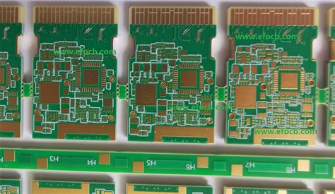
What is a Microvia PCB?
A microvia PCB is a printed circuit board that utilizes microvias, which are small holes that connect different layers of the board. These holes are typically smaller than 150 microns in diameter and are created using laser drilling or other advanced manufacturing techniques. Microvia technology allows for higher density interconnects and improved signal integrity compared to traditional through-hole or blind via designs.
Advantages of Microvia PCBs
- Increased board density
- Improved signal integrity
- Reduced layer count
- Enhanced thermal management
- Better reliability
Microvia PCB Design Considerations
When designing a microvia PCB, several factors must be taken into account to ensure optimal performance and manufacturability.
Layer Stack-up
The layer stack-up is a critical aspect of microvia PCB design. It determines the number of layers, the thickness of each layer, and the placement of microvias. A typical microvia PCB stack-up may include:
| Layer | Description |
|---|---|
| Top | Signal layer with components |
| L1 | Signal layer |
| L2 | Ground plane |
| L3 | Signal layer |
| L4 | Power plane |
| Bottom | Signal layer with components |
Via Types and Sizes
Microvias come in different types and sizes, each with its own advantages and limitations.
| Via Type | Diameter | Depth | Applications |
|---|---|---|---|
| Blind | 50-150 μm | 1-2 layers | High-density interconnects |
| Buried | 50-150 μm | 2-3 layers | High-density interconnects |
| Stacked | 50-150 μm | Multiple layers | 3D structures, package-on-package |
Signal Integrity
To maintain signal integrity in a microvia PCB, designers must consider factors such as:
- Impedance matching
- Crosstalk reduction
- Electromagnetic interference (EMI) shielding
- Grounding and power distribution
Thermal Management
Microvia PCBs generate more heat due to their higher density and smaller feature sizes. Proper thermal management techniques must be employed, such as:
- Using thermal vias to conduct heat away from components
- Incorporating heat spreaders or heat sinks
- Selecting materials with good thermal conductivity

Microvia PCB Manufacturing Process
The manufacturing process for microvia PCBs is more complex than that of traditional PCBs due to the smaller feature sizes and tighter tolerances required.
Laser Drilling
Laser drilling is the most common method for creating microvias. It uses a focused laser beam to ablate the dielectric material and create a small hole. There are two main types of laser drilling:
- CO2 laser drilling: Used for larger microvias (>100 μm) and thicker dielectric materials.
- UV laser drilling: Used for smaller microvias (<100 μm) and thinner dielectric materials.
Plating
After drilling, the microvias must be plated to create an electrical connection between layers. This is typically done using electroless copper plating followed by electrolytic copper plating.
Patterning
The copper layers are then patterned using photolithography and etching processes to create the desired circuit traces and pads.
Lamination
The individual layers are laminated together using heat and pressure to form the final PCB stack-up.

Cost Considerations for Microvia PCBs
Microvia PCBs are generally more expensive than traditional PCBs due to the advanced manufacturing processes and materials required.
Factors Affecting Cost
- Number of layers
- Board size and thickness
- Number and density of microvias
- Material selection (e.g., high-frequency laminates)
- Surface finish (e.g., ENIG, ENEPIG)
- Quantity ordered
Cost Reduction Strategies
To minimize the cost of microvia PCBs, designers can:
- Optimize the layer stack-up to reduce the number of layers and microvias required
- Use standard materials and surface finishes where possible
- Avoid unnecessary features or tight tolerances
- Consider alternative manufacturing methods, such as conductive ink printing or semi-additive processes (SAP)

Frequently Asked Questions (FAQ)
- What is the smallest microvia size that can be manufactured?
-
The smallest microvia size that can be reliably manufactured is around 50 microns in diameter. However, this may vary depending on the specific manufacturing process and equipment used.
-
Can microvias be used in high-power applications?
-
Yes, microvias can be used in high-power applications, but special considerations must be made for thermal management and current-carrying capacity. Designers may need to use multiple microvias in parallel or incorporate thermal vias to dissipate heat effectively.
-
Are microvia PCBs suitable for high-frequency applications?
-
Yes, microvia PCBs are well-suited for high-frequency applications due to their improved signal integrity and reduced parasitic effects. However, proper design techniques must be employed to minimize losses and maintain impedance matching.
-
How do microvia PCBs compare to HDI PCBs?
-
Microvia PCBs are a type of HDI (High-Density Interconnect) PCB that specifically uses microvias for layer-to-layer connections. HDI PCBs may also incorporate other features such as fine-pitch components, embedded passives, or thin dielectrics.
-
What are the reliability concerns with microvia PCBs?
- The main reliability concerns with microvia PCBs are related to the manufacturing process and the small size of the features. Incomplete plating, voids, or cracks in the microvias can lead to electrical failures or intermittent connections. Proper design, manufacturing controls, and testing can help mitigate these risks.
Conclusion
Microvia PCBs offer numerous benefits for high-density, high-performance electronic applications. By understanding the design considerations, manufacturing processes, and cost factors involved, engineers can effectively leverage this technology to create reliable and cost-effective products. As microvia PCB technology continues to evolve, it will enable even greater advances in electronic packaging and system integration.


Leave a Reply