Introduction to Kicad
Kicad is a powerful, open-source electronic design automation (EDA) software that allows users to design printed circuit boards (PCBs) from scratch. It is a cross-platform tool that runs on Windows, Linux, and macOS, making it accessible to a wide range of users. Kicad is an excellent choice for both hobbyists and professionals who want to create custom PCBs for their projects.
In this tutorial, we will cover the fundamental concepts of Kicad and guide you through the process of creating a simple PCB design. By the end of this article, you will have a solid understanding of Kicad’s basic features and be able to create your own PCB designs.
Setting Up Kicad
Installation
Before we begin, you need to install Kicad on your computer. You can download the latest version of Kicad from the official website: https://www.kicad.org/download/
Follow the installation instructions for your operating system, and once the installation is complete, launch Kicad.
Creating a New Project
When you launch Kicad, you will be greeted with the main window. To create a new project, follow these steps:
- Click on “File” in the menu bar and select “New Project.”
- Choose a location to save your project and give it a name.
- Click “Save” to create the project.
Kicad will create a new project folder containing several files, including a schematic file (.sch) and a PCB layout file (.kicad_pcb).

Schematic Design
Creating a Schematic
The first step in designing a PCB is to create a schematic. A schematic is a graphical representation of the electrical connections between components in your circuit. To create a schematic in Kicad, follow these steps:
- Double-click on the schematic file (
.sch) in the project tree to open it in the Schematic Editor. - You will see a blank schematic sheet. To add components, click on the “Place Symbol” button in the toolbar or press the “A” key on your keyboard.
- In the “Choose Symbol” dialog, browse through the libraries to find the components you need. You can also search for components by name.
- Click on a component to select it and then click on the schematic sheet to place it.
- Repeat steps 3 and 4 to add all the necessary components to your schematic.
Connecting Components
Once you have placed all the components on the schematic sheet, you need to connect them using wires. To connect components, follow these steps:
- Click on the “Place Wire” button in the toolbar or press the “W” key on your keyboard.
- Click on the first pin you want to connect and then click on the second pin to create a wire between them.
- Repeat step 2 to connect all the necessary pins.
Labeling Components
To keep your schematic organized and easy to read, it is essential to label your components. To label a component, follow these steps:
- Select the component you want to label.
- Press the “E” key on your keyboard to open the “Edit Value Field” dialog.
- Enter a name for the component (e.g., R1 for a resistor).
- Click “OK” to apply the label.

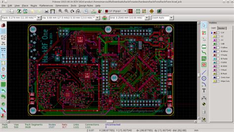
PCB Layout
Creating a PCB Layout
Once you have completed your schematic, you can create a PCB layout. A PCB layout is a physical representation of your circuit, showing the actual size and placement of components and traces. To create a PCB layout in Kicad, follow these steps:
- In the Schematic Editor, click on “Tools” in the menu bar and select “Update PCB from Schematic.”
- Kicad will generate a netlist file (
.net) and open the PCB layout file (.kicad_pcb) in the PCB Editor. - In the PCB Editor, you will see a blank PCB with the components from your schematic placed in a default arrangement.
Arranging Components
To create a functional and aesthetically pleasing PCB layout, you need to arrange the components on the board. To move a component, follow these steps:
- Select the component you want to move.
- Click and drag the component to its new location on the PCB.
- Repeat steps 1 and 2 for all the components you want to rearrange.
Routing Traces
After arranging the components, you need to connect them using traces. Traces are the copper paths that carry electrical signals between components on the PCB. To route traces, follow these steps:
- Click on the “Route Tracks” button in the toolbar or press the “X” key on your keyboard.
- Click on the first pad you want to connect and then click on the second pad to create a trace between them.
- Repeat step 2 to route all the necessary traces.
Kicad provides various routing options, such as via placement and track width adjustment, to help you create an optimal PCB layout.
Design Rule Checking (DRC)
Before finalizing your PCB layout, it is crucial to run a Design Rule Check (DRC) to ensure that your design adheres to the manufacturing constraints and design rules. To run a DRC, follow these steps:
- In the PCB Editor, click on “Inspect” in the menu bar and select “Design Rules Checker.”
- In the DRC dialog, click on “Run DRC.”
- Kicad will display any violations or errors in your PCB layout.
- Address the issues identified by the DRC and rerun the check until your design passes.

Generating Output Files
Once your PCB layout is complete and has passed the DRC, you can generate the necessary output files for manufacturing. Kicad supports various output file formats, including Gerber files, drill files, and pick-and-place files.
To generate output files, follow these steps:
- In the PCB Editor, click on “File” in the menu bar and select “Plot.”
- In the “Plot” dialog, choose the desired output file formats and specify the output directory.
- Click “Plot” to generate the output files.
You can now send these files to a PCB manufacturer to have your boards produced.
Frequently Asked Questions (FAQ)
-
Is Kicad suitable for beginners?
Yes, Kicad is an excellent choice for beginners who want to learn PCB design. It has a user-friendly interface and extensive documentation, making it easy to get started. -
Can Kicad handle complex PCB designs?
Absolutely! Kicad is a powerful tool that can handle both simple and complex PCB designs. It offers advanced features such as hierarchical sheet support, multi-sheet projects, and scripting capabilities. -
Is Kicad compatible with other EDA software?
Kicad supports various industry-standard file formats, such as Gerber files and IPC-D-356 netlist files, making it compatible with other EDA software and PCB manufacturing processes. -
Can I create custom component libraries in Kicad?
Yes, Kicad allows you to create custom component libraries. You can create new components from scratch or modify existing components to suit your needs. -
Is Kicad free to use?
Yes, Kicad is a free and open-source software released under the GNU General Public License (GPL). You can use it for personal and commercial projects without any cost.
Conclusion
Kicad is a powerful and versatile EDA software that enables users to design custom PCBs efficiently. By following this tutorial, you have learned the fundamental concepts of Kicad, including schematic design, PCB layout, and generating output files.
As you continue to work with Kicad, you will discover more advanced features and techniques that will help you create even more complex and sophisticated PCB designs. With practice and persistence, you can become proficient in using Kicad and bring your electronic projects to life.
Remember to refer to the official Kicad documentation and community resources for further guidance and inspiration. Happy PCB designing!


Leave a Reply