Table of Contents
- Introduction to KiCad
- Installing KiCad
- Creating a New Project
- Designing the Schematic
- Creating a PCB Layout
- Generating Gerber Files
- Frequently Asked Questions (FAQ)
- Conclusion
Introduction to KiCad
KiCad is a cross-platform EDA software suite that consists of several tools for designing electronic circuits and PCBs. The main components of KiCad are:
- Eeschema: Schematic editor
- Pcbnew: PCB layout editor
- Cvpcb: Footprint selector
- Gerbview: Gerber viewer
- Bitmap2Component: Converts images to footprints
KiCad supports a wide range of file formats, including KiCad’s native formats (.sch, .kicad_pcb), as well as industry-standard formats like Gerber and IPC-D-356.

Installing KiCad
To get started with KiCad, you need to download and install the software on your computer. Follow these steps to install KiCad:
- Visit the official KiCad website: https://www.kicad.org/
- Click on the “Download” button for your operating system (Windows, macOS, or Linux).
- Follow the installation instructions provided for your operating system.
Once the installation is complete, launch KiCad to verify that it is working correctly.

Creating a New Project
To create a new project in KiCad, follow these steps:
- Open KiCad and click on “File” > “New” > “Project”.
- Choose a location to save your project and give it a name.
- Click “Save” to create the project.
KiCad will create a new project folder containing the necessary files for your project.

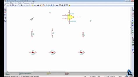
Designing the Schematic
The first step in designing a PCB is to create a schematic diagram. A schematic is a symbolic representation of the electronic circuit, showing the components and their connections. To create a schematic in KiCad, follow these steps:
- Double-click on the “Eeschema” icon in the KiCad project window to open the schematic editor.
- Use the component library to place components on the schematic by clicking on the “Place symbol” button.
- Connect the components using wires by clicking on the “Place wire” button.
- Add labels, power symbols, and other annotations as needed.
- Perform an electrical rules check (ERC) to verify the schematic for errors by clicking on the “Perform electrical rules check” button.
Once you have completed the schematic, save it and close Eeschema.
Creating a PCB Layout
After creating the schematic, the next step is to design the PCB layout. The PCB layout determines the physical placement of components and the routing of traces on the board. To create a PCB layout in KiCad, follow these steps:
- Double-click on the “Pcbnew” icon in the KiCad project window to open the PCB layout editor.
- Import the netlist generated from the schematic by clicking on “File” > “Import” > “Netlist”.
- Arrange the components on the board by moving and rotating them as needed.
- Define the board outline and place mounting holes if required.
- Route the traces between the components using the “Route tracks” tool.
- Add copper fills, text, and other graphics as desired.
- Perform a design rules check (DRC) to verify the PCB layout for errors by clicking on the “Perform design rules check” button.
Once you are satisfied with the PCB layout, save it and close Pcbnew.
Generating Gerber Files
To manufacture your PCB, you need to generate Gerber files, which are industry-standard files used by PCB fabrication companies. To generate Gerber files in KiCad, follow these steps:
- Open the PCB layout in Pcbnew.
- Click on “File” > “Plot”.
- Select the layers you want to include in the Gerber files (e.g., copper layers, solder mask, silkscreen).
- Choose the output directory and filename for the Gerber files.
- Click “Plot” to generate the Gerber files.
You can now send the generated Gerber files to a PCB fabrication company to have your PCB manufactured.
Frequently Asked Questions (FAQ)
1. Is KiCad free to use?
Yes, KiCad is a free and open-source software released under the GNU General Public License (GPL).
2. Can I use KiCad for commercial projects?
Yes, you can use KiCad for both personal and commercial projects without any licensing fees.
3. Does KiCad support 3D visualization of PCBs?
Yes, KiCad has a 3D viewer that allows you to visualize your PCB design in 3D.
4. Can I import designs from other EDA software into KiCad?
KiCad supports importing designs from various formats, including Eagle, Altium, and OrCAD. However, the quality of the import may vary depending on the complexity of the design and the compatibility of the file formats.
5. Is there a community forum or support for KiCad?
Yes, KiCad has an active community of users and developers who provide support and share knowledge through forums, mailing lists, and online resources. You can find the official KiCad forum at https://forum.kicad.info/.
Conclusion
In this comprehensive KiCad Tutorial, we have covered the essential steps for designing a PCB using KiCad, from creating a schematic to generating Gerber files for manufacturing. KiCad is a powerful and user-friendly EDA software that offers a wide range of features for electronic design. By following this step-by-step guide, you should now have a solid foundation to start creating your own PCB designs using KiCad.
Remember to refer to the official KiCad documentation and community resources for more advanced topics and techniques. With practice and experience, you will be able to create complex and professional-grade PCBs using KiCad.
| Feature | Description |
|---|---|
| Cross-platform | KiCad runs on Windows, macOS, and Linux |
| Free and open-source | Released under the GNU GPL license, allowing free use for personal and commercial projects |
| Schematic editor | Eeschema for creating schematic diagrams |
| PCB layout editor | Pcbnew for designing PCB layouts |
| 3D viewer | Visualize PCB designs in 3D |
| Gerber file generation | Generate industry-standard Gerber files for PCB manufacturing |
| Active community | Supported by a large and active community of users and developers |
Happy PCB designing with KiCad!


Leave a Reply