Introduction to KiCAD and Rayming
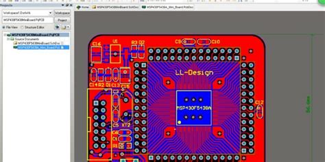
KiCAD is an open-source electronic design automation (EDA) software that allows users to design printed circuit boards (PCBs) from schematic capture to PCB layout. It has gained popularity among hobbyists, students, and professionals due to its free availability and robust features.
Rayming is a company that specializes in PCB manufacturing and assembly services. They have recently introduced a new feature that enables their system to read native KiCAD data directly, eliminating the need for users to convert their designs into different formats before submitting them for manufacturing.
Benefits of Rayming’s Native KiCAD-Data Support
Streamlined PCB Manufacturing Process
By supporting native KiCAD data, Rayming has streamlined the PCB manufacturing process for KiCAD users. Designers no longer need to spend time converting their KiCAD designs into other formats like Gerber or ODB++. This saves valuable time and reduces the chances of errors occurring during the conversion process.
Preserving Design Integrity
When converting PCB designs from one format to another, there is always a risk of losing important information or introducing errors. Rayming’s native KiCAD-data support ensures that the original design remains intact throughout the manufacturing process. This preserves the integrity of the design and minimizes the likelihood of manufacturing issues.
Faster Turnaround Times
With Rayming’s ability to read native KiCAD data, the time required for PCB manufacturing is significantly reduced. Designers can submit their KiCAD files directly to Rayming, and the manufacturing process can begin immediately. This faster turnaround time allows for quicker prototyping and shorter product development cycles.

How to Submit KiCAD Designs to Rayming
Submitting KiCAD designs to Rayming for manufacturing is a straightforward process. Follow these steps to ensure a smooth submission:
- Complete your PCB design in KiCAD, ensuring that all components, traces, and layers are properly defined.
- Generate the necessary output files from KiCAD, including the PCB layout file (.kicad_pcb) and the schematic file (.sch).
- Package the KiCAD project folder, including all related files, into a compressed archive (e.g., ZIP or RAR).
- Visit the Rayming website and navigate to the PCB submission page.
- Fill out the required information, such as your contact details, project specifications, and desired quantities.
- Upload the compressed KiCAD project folder to the Rayming website.
- Review your submission and provide any additional instructions or requirements.
- Submit your order and wait for Rayming to process your KiCAD design files.
| Step | Description |
|---|---|
| 1 | Complete your PCB design in KiCAD |
| 2 | Generate necessary output files (.kicad_pcb and .sch) |
| 3 | Package the KiCAD project folder into a compressed archive |
| 4 | Visit the Rayming website and navigate to the PCB submission page |
| 5 | Fill out the required information and project specifications |
| 6 | Upload the compressed KiCAD project folder |
| 7 | Review your submission and provide additional instructions |
| 8 | Submit your order and wait for Rayming to process your KiCAD files |

Advantages of Using KiCAD for PCB Design
Cost-Effective Solution
KiCAD is a free and open-source EDA software, making it an attractive option for individuals and small businesses with limited budgets. Unlike proprietary EDA tools that often come with high licensing costs, KiCAD allows users to design PCBs without any financial burden.
Cross-Platform Compatibility
KiCAD is available for multiple operating systems, including Windows, macOS, and Linux. This cross-platform compatibility ensures that designers can work on their PCB projects regardless of their preferred computing environment. It also facilitates collaboration among team members who may be using different platforms.
Active Community Support
KiCAD has a vibrant and active community of users and developers who contribute to its development, provide support, and share their knowledge. The community offers forums, tutorials, and resources that help users navigate the software and overcome design challenges. This strong community support ensures that KiCAD users can find assistance whenever they need it.
Extensive Component Libraries
KiCAD comes with an extensive library of components that designers can use in their PCB projects. These libraries include a wide range of common electronic components, such as resistors, capacitors, integrated circuits, and connectors. Additionally, users can create custom component libraries or import libraries from other sources, further expanding the available component options.
Schematic Capture and PCB Layout Integration
KiCAD provides a seamless integration between schematic capture and PCB layout. Designers can create their circuit schematics using the Eeschema tool and then seamlessly transfer the design information to the PCB layout tool, Pcbnew. This integration ensures consistency between the schematic and the PCB layout, reducing the chances of errors and improving the overall design process.

Frequently Asked Questions (FAQ)
1. Is Rayming’s native KiCAD-data support available for all PCB manufacturing services?
Yes, Rayming’s native KiCAD-data support is available for all their PCB manufacturing services, including prototype and production runs.
2. Can I still use other PCB design software and submit my designs to Rayming?
Yes, Rayming accepts PCB design files from other EDA software as well. However, using KiCAD and submitting native KiCAD data offers the benefits of a streamlined process and preserved design integrity.
3. Are there any limitations on the complexity of KiCAD designs that Rayming can manufacture?
Rayming can handle a wide range of PCB complexities, from simple single-layer boards to complex multi-layer designs. However, it’s always best to consult with Rayming’s technical support team to ensure that your specific design requirements can be met.
4. How long does it typically take for Rayming to manufacture PCBs from KiCAD designs?
The manufacturing time depends on various factors, such as the complexity of the design, the selected manufacturing options, and the current workload at Rayming. Typically, prototype runs can be completed within a few days, while production runs may take longer. Rayming provides estimated lead times for each project.
5. Can I request modifications to my KiCAD design after submitting it to Rayming?
Yes, you can request modifications to your KiCAD design after submission. However, it’s important to communicate any changes as soon as possible to avoid delays in the manufacturing process. Rayming’s technical support team will work with you to accommodate any necessary modifications.
Conclusion
Rayming’s native KiCAD-data support is a game-changer for KiCAD users, offering a streamlined PCB manufacturing process, preserved design integrity, and faster turnaround times. By eliminating the need for file format conversions, Rayming has simplified the PCB manufacturing workflow for KiCAD designers.
KiCAD itself is a powerful and cost-effective EDA software that provides a comprehensive suite of tools for schematic capture and PCB layout. Its cross-platform compatibility, active community support, extensive component libraries, and seamless integration between schematic and layout make it an attractive choice for PCB designers.
With Rayming’s native KiCAD-data support, designers can leverage the benefits of KiCAD and enjoy a smooth and efficient PCB manufacturing experience. Whether you are a hobbyist working on personal projects or a professional designing complex PCBs, Rayming’s KiCAD-Rayming integration offers a reliable and streamlined solution for bringing your designs to life.


Leave a Reply