Introduction
Flexible printed circuit boards (flex PCBs or flex circuits) are a type of PCB that incorporate flexible dielectric materials such as polyimide or polyester. This allows the circuit board to bend and flex while still maintaining electrical connectivity. Flex PCBs have many advantages over traditional rigid PCBs including:
- Bendability – can conform to 3D shapes and allow for complex packaging and interconnects
- Vibration/shock resistance – the flexibility absorbs stresses that would damage a rigid board
- Light weight – thinner flexible materials reduce weight vs FR4
- High layer count – more layers allow increased routing density
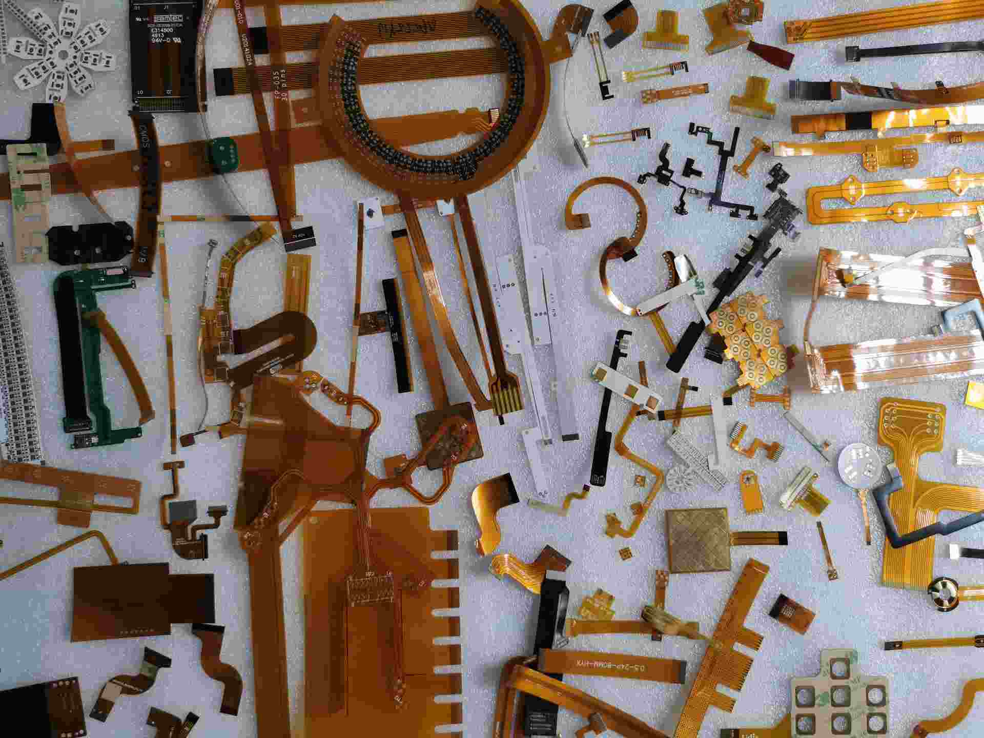
Some common applications of flex PCBs include computer displays, mobile devices, automotive electronics, aerospace avionics, and medical devices. The flexible nature allows the PCB to move dynamically in these products.
Kicad is an open-source electronic design automation (EDA) software suite that can be used to design both rigid and flexible PCBs. This article will provide an overview of using Kicad for designing flex circuits, including layout, routing, documentation, and fabrication outputs.
Designing Flex PCBs in Kicad
The overall workflow for designing a flex PCB in Kicad is similar to that of rigid PCBs:
- Schematic capture
- PCB layout
- Stackup definition
- Component placement
- Trace routing
- Specifying flex areas
- Generate fabrication outputs
However, there are some key considerations and differences when working with flex PCBs in Kicad.
Selecting Flexible Materials
The first step is selecting the appropriate flex materials to use in the PCB stackup. Common base dielectric materials include:
- Polyimide (Kapton) – most popular flex material, high temp resistance
- Polyester (PET) – lower cost, not as heat resistant as polyimide
- PEN – similar properties as polyimide, but more flexible
The copper layers are bonded to the dielectric layers with acrylic or epoxy adhesives. Flex-rigid boards often incorporate standard FR4 layers alongside the flexible layers.
Kicad includes predefined flex stackups, but also allows fully custom user-defined selections. The material properties like dielectric constant and loss tangent can be configured.
Flex Area Keepouts
Once the stackup is defined, layout of components and traces proceeds as normal. However, it is important to clearly delineate sections of the PCB that should remain rigid and areas that are allowed to flex.
This is done by drawing keepout lines around rigid sections using the “Keepout” layer in Kicad. Any area outside the keepouts is considered a “flex area” that will utilize the flexible materials.
Example of a rigid area keepout on a flex PCB
It is best practice to minimize the number of rigid sections and maximize flex areas for optimal bendability. The rigid sections can be used for connectors, chips, and other stiff components.
Bend Radii
In flex areas, it is important to account for mechanical stability when bending. Sharp corners and small radii can cause excessive stress.
For this reason, traces should avoid acute angles less than 90 degrees in flex sections. Instead, utilize curved traces with sufficient bend radii.
Kicad includes constraints for the minimum bend radius based on the stackup materials and copper weight. The PCB editor will ensure traces do not violate the minimum bend constraints.
Routing and Vias
Routing traces in the flex areas requires following best practices like:
- Avoid acute angles less than 90 degrees
- Minimize length of traces in bend areas
- Stagger traces to prevent overlaps when bent
- Longer traces should be routed in zig-zag or serpentine patterns
- Ensure adequate bend radius on traces
Vias act as points of rigidity and should be avoided in bend areas when possible. Where needed, staggered arrangement helps prevent cracking. Microvias minimize stress.
Flex-Rigid Interconnect
Connecting rigid and flex sections requires careful attention to the transitional area. Strategies like teardrops, rounded pads, and matching radii help reduce stresses.
If possible, avoid routing high speed signals across the rigid-flex junction. Filters may be needed for sensitive traces.
Documentation and Fabrication
Once the flex PCB layout is completed in Kicad, documentation and fabrication files can be generated.
Documentation
Kicad can produce industry standard drawings used for documentation and fabrication. This includes:
- Schematic PDF
- Assembly Drawings
- Fabrication Drawings
- Drill Drawing
- Gerber files
The fabrication drawings are especially important for flex PCBs, since they clearly show the rigid areas vs flex sections.
Fabrication Outputs
In addition to documentation, Kicad can export all the necessary files needed to fabricate the board:
- Gerber files – used for photoploting copper layers
- Excellon drill files – NC drill toolpaths
- IPC-2581 archive – alternative to Gerber, contains all fabrication data in one file
The IPC-2581 format is becoming more popular, as it streamlines transferring PCB data to manufacturers.
Ensure the fabrication outputs align with the requirements of your PCB manufacturer. Most flex PCB vendors accept the standard Gerber and Excellon formats.
Flex PCB Guidelines and Limitations
When designing flex circuits, keep these guidelines and limitations in mind:
- Minimum trace/space is typically 6mil (0.15mm)
- Minimum insulation width around exposed pads is 6mil
- Vias can crack if not reinforced – use microvias
- Matching impedances often requires wider traces
- High frequency signals may require shielding
- Components leads must be formed to absorb flexing forces
- Avoid components in high flex areas if possible
- Adhesives may be required to anchor stiff components
Following best practices for flex PCB layout will help ensure the board bends properly and maintains reliability. Finding a fabricator experienced in building flex boards is also recommended.
Conclusion
Kicad provides the capabilities necessary for designing flexible PCBs, from stackup definition through final fabrication outputs. While requiring additional considerations compared to rigid boards, flex circuits enable creative solutions not otherwise possible. Utilizing the guidelines outlined in this article will set your next flex PCB project up for success.
The combination of Kicad’s powerful features and the unique merits of flex PCB technology offers electronics designers expanded options for solving challenging problems across many fields and applications.
FQA
Here are some frequently asked questions and answers about designing flex PCBs in Kicad:
Q: What are some typical stackups used for flex PCBs?
A: Common flex stackups are single layer (1 copper + 1 dielectric), 2 layer (2 copper + 1 dielectric), and multilayer with 4-8 copper layers. Dielectric materials are usually polyimide or polyester in various thicknesses (1mil to 5mil).
Q: How do I model different bend radii in Kicad?
A: The Radius setting under the Bend Constraints section of the Design Rules allows configuring the minimum bend radius. This can be set globally or per net class.
Q: Can I do impedance controlled routing in flex regions?
A: Yes, you can define impedance profiles and use the interactive length tuning to match target impedances when routing in flex areas, just like in rigid sections. This may require wider than typical trace widths.
Q: Are there special considerations for components mounted in flex regions?
A: Use only flex-compatible components rated for dynamic bending. Through-hole parts must have leads formed in a U-shape to allow flexing without damage. Adhesives may be needed to reinforce parts.
Q: What fab layer requirements are unique to flex PCB manufacturing?
A: You’ll need to provide the mechanical layer drawing showing rigid areas vs. flex sections. The min bend radius also needs to be specified based on the material. Let your manufacturer know it is a flex board.


Leave a Reply