What is a J111 JFET?
The J111 is a type of Junction Field Effect Transistor (JFET) that is commonly used in electronic circuits. It is an N-channel depletion-mode device, meaning that it is normally on (conducting) when there is no voltage applied to its gate terminal. The J111 is known for its high input impedance, low noise, and excellent temperature stability, making it suitable for a wide range of applications.
Key Features of the J111 JFET
| Feature | Description |
|---|---|
| N-channel | Conducts current through an N-type semiconductor channel |
| Depletion-mode | Normally on (conducting) when no gate voltage is applied |
| High input impedance | Minimal current drawn by the gate terminal |
| Low noise | Generates less noise compared to bipolar junction transistors |
| Temperature stability | Maintains consistent performance over a wide temperature range |
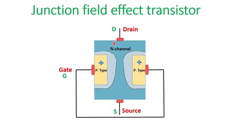
J111 JFET Pinout and Package
The J111 JFET is available in various package types, with the most common being the TO-92 package. The TO-92 package is a small, three-lead plastic package that is easy to handle and solder.
J111 JFET TO-92 Package Pinout
| Pin Number | Pin Name | Description |
|---|---|---|
| 1 | Source | The source terminal of the JFET |
| 2 | Gate | The gate terminal, controls the channel conductivity |
| 3 | Drain | The drain terminal of the JFET |

How Does a J111 JFET Work?
A J111 JFET operates by controlling the current flow through a semiconductor channel between the source and drain terminals. The conductivity of this channel is modulated by the voltage applied to the gate terminal.
J111 JFET Operation Modes
-
Depletion Mode: When no voltage is applied to the gate (VGS = 0), the J111 is in depletion mode, and the channel is fully open, allowing maximum current to flow between the source and drain.
-
Pinch-off Mode: As the gate-to-source voltage (VGS) becomes more negative, the depletion region widens, narrowing the channel and reducing the current flow. At a certain negative VGS, called the pinch-off voltage (Vp), the channel is completely closed, and no current flows between the source and drain.
J111 JFET Transfer Characteristic Curve
The transfer characteristic curve of a J111 JFET shows the relationship between the drain current (ID) and the gate-to-source voltage (VGS) at a constant drain-to-source voltage (VDS).
As the graph illustrates, when VGS is 0 V (depletion mode), the drain current is at its maximum (IDSS). As VGS becomes more negative, the drain current decreases until it reaches zero at the pinch-off voltage (Vp).

J111 JFET Applications
The J111 JFET is used in a variety of electronic circuits due to its unique characteristics and benefits. Some common applications include:
-
Amplifiers: J111 JFETs are often used in low-noise, high-input impedance amplifier stages, such as in audio and instrumentation applications.
-
Switches: J111 JFETs can be used as voltage-controlled switches, taking advantage of their ability to control current flow with a small gate voltage.
-
Voltage-controlled resistors: J111 JFETs can be used as voltage-controlled resistors in circuits such as voltage-controlled filters and voltage-controlled oscillators.
-
Current sources: J111 JFETs can be configured as constant current sources, providing a stable current over a wide range of load impedances.
-
Temperature sensors: The J111 JFET’s temperature stability makes it suitable for use in temperature sensing applications, where its characteristics change predictably with temperature.

Biasing a J111 JFET
To operate a J111 JFET correctly, it must be properly biased. Biasing involves setting the appropriate DC voltages and currents at the device’s terminals to ensure that it functions in the desired operating region.
Common J111 JFET Biasing Configurations
- Self-bias: In this configuration, a resistor is connected between the source and ground, creating a voltage drop that automatically biases the gate-to-source voltage (VGS) to the proper operating point.
- Voltage-divider bias: This configuration uses a voltage divider network connected to the gate to set the desired VGS. The voltage divider provides a more stable bias point compared to the self-bias configuration.
- Current-source bias: In this configuration, a constant current source is connected to the source terminal, providing a stable bias current and minimizing the impact of device parameter variations.
J111 JFET Small-signal Model
To analyze the behavior of a J111 JFET in a circuit, a small-signal model is often used. This model represents the device’s characteristics when operating with small AC signals superimposed on the DC bias point.
J111 JFET Small-signal Model Parameters
| Parameter | Description |
|---|---|
| gm | Transconductance, relates the change in drain current to the change in gate-to-source voltage |
| rd | Dynamic drain-to-source resistance |
| Cgs | Gate-to-source capacitance |
| Cgd | Gate-to-drain capacitance |
The small-signal model helps designers analyze the J111 JFET’s performance in various circuit configurations, such as amplifiers and filters.
J111 JFET Datasheet and Specifications
When designing circuits using the J111 JFET, it is crucial to consult the device’s datasheet for detailed specifications and recommended operating conditions. The datasheet provides information such as:
- Maximum ratings (e.g., maximum drain-to-source voltage, maximum gate-to-source voltage, maximum power dissipation)
- Electrical characteristics (e.g., drain-to-source on-resistance, gate-to-source cutoff voltage, transconductance)
- Typical performance graphs (e.g., transfer characteristic, drain current vs. drain-to-source voltage)
- Package dimensions and pinout
By carefully reviewing the datasheet, designers can ensure that they are using the J111 JFET within its specified limits and optimizing its performance in their circuits.
Frequently Asked Questions (FAQ)
- What is the difference between a JFET and a MOSFET?
-
A JFET (Junction Field Effect Transistor) has a channel made of N-type or P-type semiconductor material, and its conductivity is controlled by a reverse-biased PN junction. In contrast, a MOSFET (Metal Oxide Semiconductor Field Effect Transistor) has a channel that is controlled by an electric field generated by a voltage applied to an insulated gate terminal.
-
Can a J111 JFET be used as an amplifier?
-
Yes, the J111 JFET is commonly used in amplifier circuits, particularly in low-noise, high-input impedance applications such as audio and instrumentation amplifiers.
-
What is the pinch-off voltage of a J111 JFET?
-
The pinch-off voltage (Vp) of a J111 JFET is the gate-to-source voltage at which the drain current becomes zero. The exact value of Vp can vary between devices and is specified in the device’s datasheet.
-
How do I properly bias a J111 JFET?
-
To properly bias a J111 JFET, you can use one of several biasing configurations, such as self-bias, voltage-divider bias, or current-source bias. The choice of biasing configuration depends on the specific circuit requirements and the desired operating point of the JFET.
-
What are the advantages of using a J111 JFET over a bipolar junction transistor (BJT)?
- Compared to BJTs, J111 JFETs offer several advantages, including:
- Higher input impedance, which means they draw less current from the input signal source
- Lower noise, making them suitable for low-noise applications
- Better temperature stability, maintaining consistent performance over a wide temperature range
- Simpler biasing requirements, as they do not require a continuous base current to operate
In summary, the J111 JFET is a versatile and widely-used semiconductor device that offers unique characteristics and benefits in various electronic circuits. By understanding its pinout, features, applications, and biasing requirements, designers can effectively utilize the J111 JFET to create high-performance, low-noise, and temperature-stable circuits.


Leave a Reply