Introduction to Irf540 Pinout
The IRF540 is a popular N-channel MOSFET (Metal-Oxide-Semiconductor Field-Effect Transistor) widely used in various electronic applications. It is known for its high power handling capability, fast switching speed, and low on-resistance. Understanding the IRF540 pinout is crucial for properly integrating this MOSFET into your circuits and harnessing its full potential.
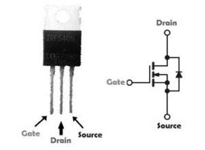
Irf540 Pinout Diagram
The IRF540 comes in a TO-220 package, which is a common through-hole package for power devices. The package has three pins: Gate (G), Drain (D), and Source (S). Here’s a visual representation of the IRF540 pinout:
         +---------+
         |         |
         |   IRF540|
         |         |
    G ---| 1     3 |--- D
         |    2    |
    S ---|         |
         |         |
         +---------+
| Pin Number | Pin Name | Description |
|---|---|---|
| 1 | Gate (G) | Controls the switching of the MOSFET |
| 2 | Source (S) | Connected to the negative side of the load |
| 3 | Drain (D) | Connected to the positive side of the load |

Working Principle of Irf540
The IRF540 is an enhancement-mode MOSFET, which means it is normally off when no voltage is applied to the gate. To turn on the MOSFET, a positive voltage must be applied to the gate, creating an electric field that attracts electrons to form a conductive channel between the drain and source.
Irf540 as a Switch
One of the primary applications of the IRF540 is as a high-speed, low-loss switch. When a sufficient positive voltage (typically 10V or higher) is applied to the gate, the MOSFET turns on, allowing current to flow from the drain to the source. When the gate voltage is removed or falls below the threshold voltage, the MOSFET turns off, blocking current flow.
Irf540 as a Variable Resistor
The IRF540 can also be used as a variable resistor by operating it in the linear region. By applying a varying voltage to the gate, you can control the resistance between the drain and source, allowing you to regulate the current flow. This property is useful in applications such as voltage regulators and motor speed control.

Key Features of Irf540
The IRF540 boasts several impressive features that make it a popular choice for power electronics applications:
-
High Current Handling: The IRF540 can handle continuous drain currents up to 33A, making it suitable for high-power applications.
-
Low On-Resistance: With a typical on-resistance of just 0.044Ω, the IRF540 minimizes power losses and ensures efficient power delivery.
-
Fast Switching Speed: The IRF540 has fast switching times, with a typical rise time of 44ns and a fall time of 43ns, enabling high-frequency operation.
-
Wide Operating Voltage Range: The MOSFET can handle drain-to-source voltages up to 100V, providing flexibility in circuit design.
-
Robust Protection: The IRF540 features built-in protection against electrostatic discharge (ESD) and transient voltage spikes, enhancing its reliability.

Applications of Irf540
The IRF540 finds use in a wide range of electronic applications, including:
-
Power Supplies: The IRF540 is commonly used in switch-mode power supplies (SMPS) as a high-efficiency switching element.
-
Motor Drivers: Thanks to its high current handling capability, the IRF540 is well-suited for driving DC motors, stepper motors, and brushless motors.
-
Inverters and Converters: The MOSFET’s fast switching speed and low losses make it ideal for use in power inverters and DC-DC converters.
-
Lighting Control: The IRF540 can be employed in LED drivers and dimming circuits to control the brightness of LED lighting systems.
-
Automotive Electronics: The IRF540’s robustness and high power handling make it suitable for automotive applications such as fuel injection systems and motor control.
Irf540 Specifications
Here are some key specifications of the IRF540:
| Parameter | Value |
|---|---|
| Maximum Drain-to-Source Voltage (VDSS) | 100V |
| Maximum Continuous Drain Current (ID) | 33A |
| Maximum Gate-to-Source Voltage (VGS) | ±20V |
| Threshold Voltage (VGS(th)) | 2V to 4V |
| Static Drain-to-Source On-Resistance (RDS(on)) | 0.044Ω |
| Input Capacitance (Ciss) | 1960pF |
| Output Capacitance (Coss) | 360pF |
| Reverse Transfer Capacitance (Crss) | 120pF |
| Total Gate Charge (Qg) | 72nC |
Irf540 vs Other MOSFETs
When comparing the IRF540 to other MOSFETs, it’s essential to consider factors such as voltage and current ratings, on-resistance, switching speed, and package type. Here’s a comparison of the IRF540 with a few other popular MOSFETs:
| MOSFET | VDSS | ID | RDS(on) | Package |
|---|---|---|---|---|
| IRF540 | 100V | 33A | 0.044Ω | TO-220 |
| IRFZ44N | 55V | 49A | 0.028Ω | TO-220 |
| IRF3205 | 55V | 110A | 0.008Ω | TO-220 |
| IRLZ44N | 55V | 47A | 0.022Ω | TO-220 |
Choose the MOSFET that best suits your application requirements, considering the trade-offs between voltage and current ratings, on-resistance, and cost.
Irf540 Circuit Design Considerations
When designing circuits with the IRF540, keep the following considerations in mind:
-
Gate Drive Requirements: Ensure that your gate driver can provide sufficient voltage and current to fully turn on the MOSFET. A gate voltage of 10V or higher is typically required.
-
Heat Dissipation: The IRF540 can generate significant heat during operation, especially when handling high currents. Use an appropriate heatsink and thermal management techniques to prevent overheating.
-
Snubber Circuits: In high-speed switching applications, consider using snubber circuits to suppress voltage and current spikes that can damage the MOSFET.
-
Paralleling MOSFETs: If higher current handling is needed, you can parallel multiple IRF540s. However, ensure proper current sharing by using balancing resistors and matching the MOSFETs’ characteristics.
-
PCB Layout: Optimize your PCB layout to minimize stray inductance and capacitance, which can cause ringing and oscillations. Keep the gate, drain, and source traces short and wide to reduce parasitic effects.
Frequently Asked Questions (FAQ)
- What is the maximum voltage that can be applied to the IRF540’s drain?
-
The maximum drain-to-source voltage (VDSS) for the IRF540 is 100V. Exceeding this voltage can cause permanent damage to the MOSFET.
-
How much current can the IRF540 handle?
-
The IRF540 can handle a maximum continuous drain current (ID) of 33A. However, the actual current handling capability depends on factors such as the heatsink, ambient temperature, and duty cycle.
-
What is the purpose of the gate resistor in an IRF540 circuit?
-
The gate resistor serves two primary purposes: it limits the current flowing into the gate during switching, preventing damage to the MOSFET, and it helps to suppress high-frequency oscillations and ringing.
-
Can the IRF540 be used for AC switching applications?
-
While the IRF540 is primarily designed for DC switching applications, it can be used in AC switching circuits with appropriate snubber networks and zero-crossing detection techniques.
-
How do I choose the right heatsink for my IRF540?
- The selection of a heatsink depends on factors such as the power dissipation, ambient temperature, and desired MOSFET temperature. Use the thermal resistance values provided in the IRF540 datasheet to calculate the required heatsink rating. Online heatsink calculators and simulation tools can also assist in the selection process.
Conclusion
The IRF540 is a versatile and reliable N-channel MOSFET that finds widespread use in power electronics applications. Its high current handling capability, low on-resistance, and fast switching speed make it an excellent choice for switching and linear regulation purposes. By understanding the IRF540 pinout, working principle, and key features, you can effectively integrate this MOSFET into your circuits and harness its performance advantages. When designing with the IRF540, pay attention to gate drive requirements, heat dissipation, and proper PCB layout techniques to ensure optimal operation and long-term reliability.


Leave a Reply